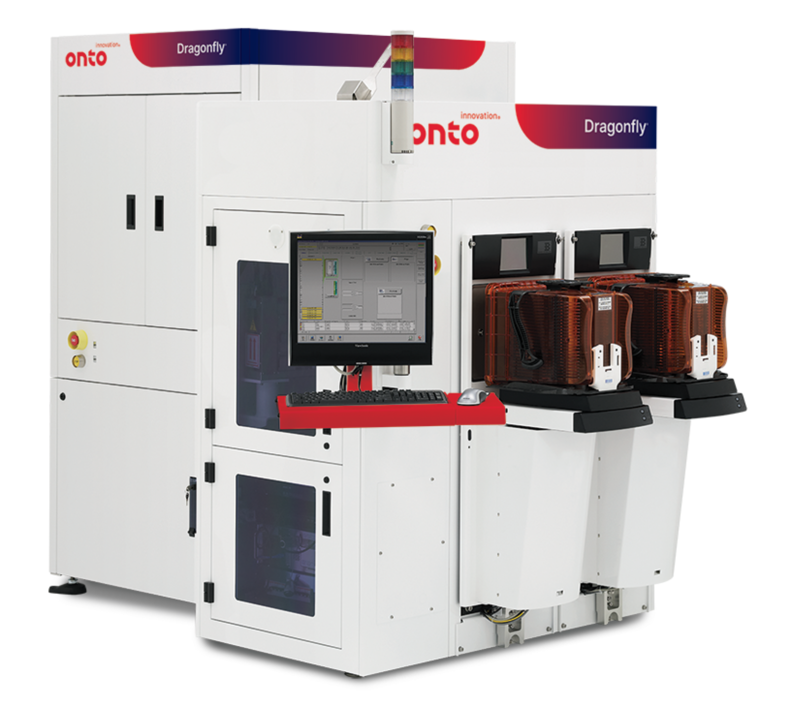
Product Overview
Unique 2D imaging technology provides fast, reliable inspection for sub-micron defects to meet today's R&D needs and tomorrow's production demands. Onto Innovation's 3Di™ technology delivers precision bump height metrology and coplanarity. This new technology is the foundation of Onto Innovation’s products designed to offer fast throughput, increased brightfield and darkfield sensitivity and solves site challenges related to large package inspection.
The Dragonfly G3 system offers Clearfind® Technology for non-visual residue detection. For specialty markets, such as CMOS image sensors (CIS), the Dragonfly System uses a combination of oblique angle illumination with sophisticated image processing and a machine-learning algorithm to detect low contrast defects in the active pixel sensor area.
The Dragonfly G3 system is tightly integrated with control and analytical software for real-time analysis and review, high speed IR defect inspection and review, while also providing offline review options. When massive amounts of bump data are generated during inspection, users now have the tools to visualize data, correlate process variations and improve yields through exploratory data analysis down to the bump level.

Applications
- Micro bumps
- After develop and etch
- Large die, multi-chip packages
- Reconstituted wafers
- Redistribution layers (RDL)
- OQA and post saw
- CMOS image sensor (CIS)
- Gel and waffle pack inspection
- Multi-product, multi-grid
- MEMS
- Post Probe
Specifications
- Inline real-time focusing
- Flexible platform to allow for metrology sensor integration
- High speed IR defect inspection and review
- Large die and package support (>6400mm2)
- Substrate support: 100mm - 330mm wafers
- Substrate handling: wafer, frame, warped, thin, waffle pack, porous
- High warped wafer and Taiko handling options
- Waferless recipe creation using automated alignment and CAD import
- Native tool matching and recipe sharing with common recipe server
- Rule based binning and classification for immediate die disposition
- Online and offline review capability
- Integrated backside and edge inspection (option)
- AI ADC and yield management software (option)