Memory 

Our digital world generates an enormous amount of data that is stored locally on a device or in the cloud. Memory has become the cornerstone of the mobile world and one of the most critical semiconductor devices manufactured today.

3D NAND Process Control

Hardmask, HAR channel hole and slit etch profile metrology for real-time process feedback

As the number of layers in 3D NAND increases, hardmasks are used for etching deep, high aspect ratio (HAR) features that conventional photoresists cannot withstand. Monitoring hard mask thickness is critical to the 3D NAND process as it goes through an iterative etch process. Film thickness and repeatability affects the active area of cell and consistency of the litho/etch performance. Improved device performance and yield rely on the ability to accurately measure these layers and understand the correlation to the deposition and etch processes.

In addition, etching HAR features like channel hole and slit (word line cut) is posing a large challenge in 3D NAND process control. Monitoring HAR hole and trench profile and tilt/twist is critical to the 3D NAND process as an uncontrolled etch profile variation causes device short, reduced channel mobility and loss of yield. The ability to accurately measure the HAR etch profile for real-time process control is critical to device performance and yield.
DRAM High Bandwidth Memory TSV

Inspection and metrology for stacked die

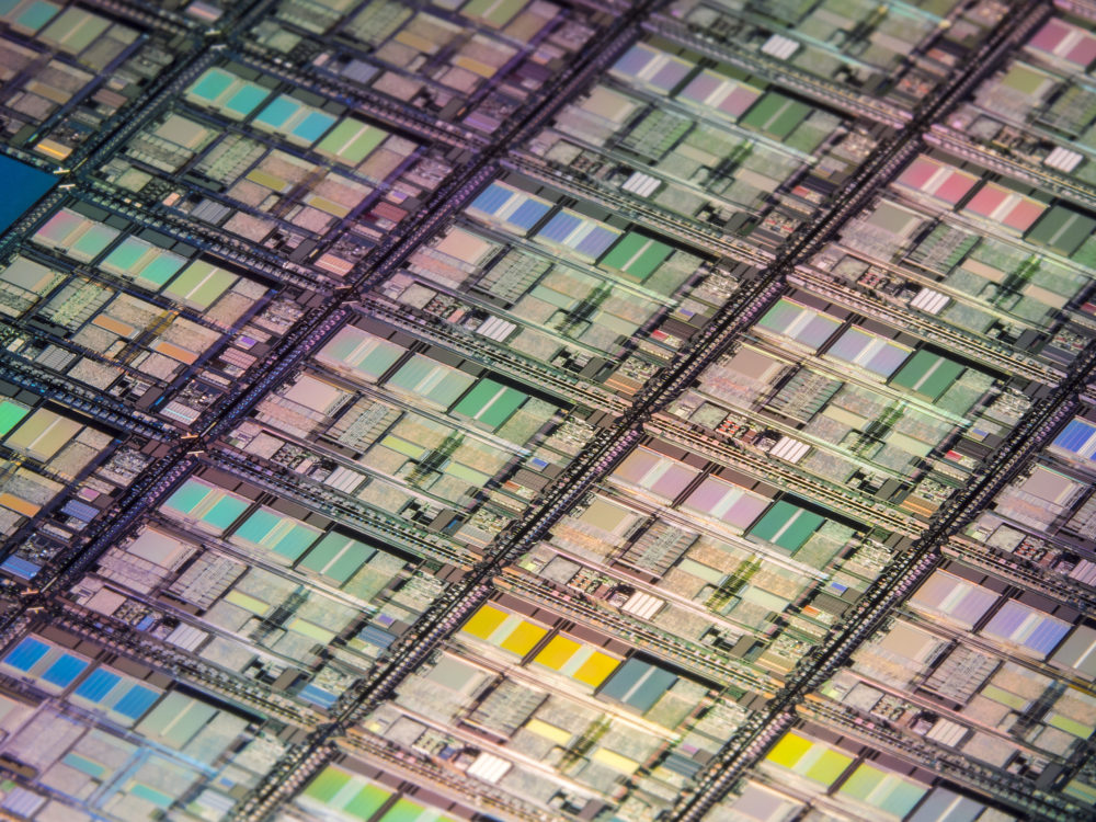
High bandwidth memory (HBM) is achieved by the stacking of individual DRAM die. This stacking is made possible through the use of through silicon vias (TSVs). The inspection and CD metrology of these vias is necessary to ensure the interconnects between the die are successfully aligned and in contact with each other. In addition, the microbumps on the die being stacked need to be inspected to ensure interconnect coplanarity.

DRAM Front-end Process Control

DRAM scaling toward D1α and D1β nodes

With continuous scaling of DRAM toward D1α and D1β nodes, process control for buried word line fin height/CD, bit line contact bottom CD/recess, high aspect ratio (HAR) capacitor etch profile, as well as overlay shifts between active areas, word lines, bit lines, bit line contacts, and capacitors has become more challenging than ever. Device performance is highly dependent on the accurate control of these dimensions with smaller error budget.

The ability to accurately measure DRAM front-end CDs, overlays, and HAR profiles for process control is critical to DRAM device performance and yield.

Consulting and Applications Services

Onto Innovation's process control consulting services allow busy manufacturers to focus on production while we examine how to improve the process.

The Onto Innovation applications teams have over twenty years of experience with hundreds of successful projects worldwide across multiple industries. Contact us today to discuss your application study needs.

Contact Us

You Have
a Challenge? We Love
a Challenge.

Let's Talk