ENHANCED CAPABILITY TO ELIMINATE DEFECT ESCAPE
Due to growing consumer demand for mobile phones, tablets, wearable devices and the Internet of Things (IoT), the semiconductor industry continues its evolution from wafer level chip scale packaging (WLCSP) to fan-out wafer level packaging (FOWLP) and 2.5D and 3D processing.
Cost remains the main driver and high yields are mandatory as the industry continues to drive down defectivity rates. As the processes for these advanced packaging products take on a more fab-like look, and are implemented in what is now being called the middle-end, attention is turning to defects that are normally not visible. Examples of non-visible defects range from voids in through silicon vias (TSVs) to faint organic photoresist or cleaning chemical residues and incomplete etch on the bump pad. These organic contaminants are often the root cause of field failures, which occur after the material has been exposed to operating conditions for extended periods.
A comprehensive process control strategy for a complex advanced packaging flow requires multiple inspection and metrology approaches.
Organic defects have been tedious to detect using manual microscopes
These classes of contaminants and residues can escape detection under conventional white light (brightfield or darkfield) illumination schemes, creating a need for innovative illumination modes that highlight these types of defects. Such an approach could also be useful in distinguishing low contrast organic defects from the high contrast grain structure of underlying metals, or conversely, in finding shorts or opens in metal lines that overlay highlighted organic layers.
Additionally, nuisance defects (false positives that should be ignored) are particularly costly in the back-end where the sunk cost of each finished, known-good-die (KGD) is extraordinarily high. The intelligent combination of multiple illumination modes, sophisticated segmentation algorithms and automatic defect classification could greatly reduce the number of nuisance defects, eliminating costly and unnecessary product losses.
Uncover non-visible defects.
Onto Innovation has devised a way to detect non-visible defects using Clearfind® technology. Clearfind technology incorporates high sensitivity camera sensor technology, a dual inline focus system, and patented illumination. It includes a coarse z focus system that allows the optics to stay in the optimum focus range while a fine focus system continuously measures the local topography as it scans the wafer and adjusts focus automatically.
This unique methodology allows Clearfind technology to rapidly move the imaging objective and slowly move the optical head to maintain sharp imagery throughout the inspection. Maintaining focus is critical for high-resolution inspection of highly warped wafers. Using Clearfind technology, the system is capable of capturing organic defects at or below 1µm.
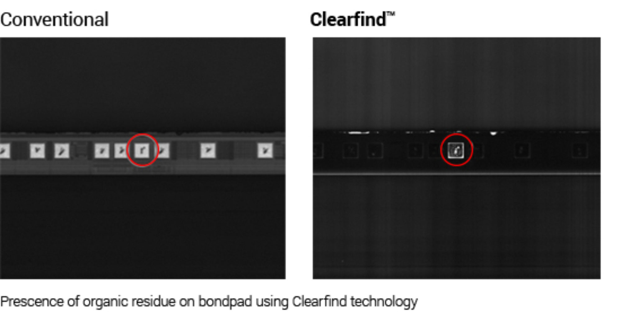
The images below were captured using brightfield and Clearfind technology respectively. The brightfield image requires an advanced algorithm to detect these low contrast defects. This advanced algorithm could result in nuisance defects in other parts of the device requiring advanced binning and filtering to only capture the critical defect. However, using Clearfind technology, the same low-contrast organic defect shows more than 10 times the contrast as seen with the standard technology. This allow the inspection system to use a simple threshold-based algorithm to detect these defects without the need of advanced binning and filtering of nuisance defects.

In the following images, no defects are detected on the bondpad using standard brightfield illumination. However, when we inspect the same device using Clearfind technology, we could see residue on one of the bondpads. This residue could cause subsequent failure during electrical test or even a costlier field failure.

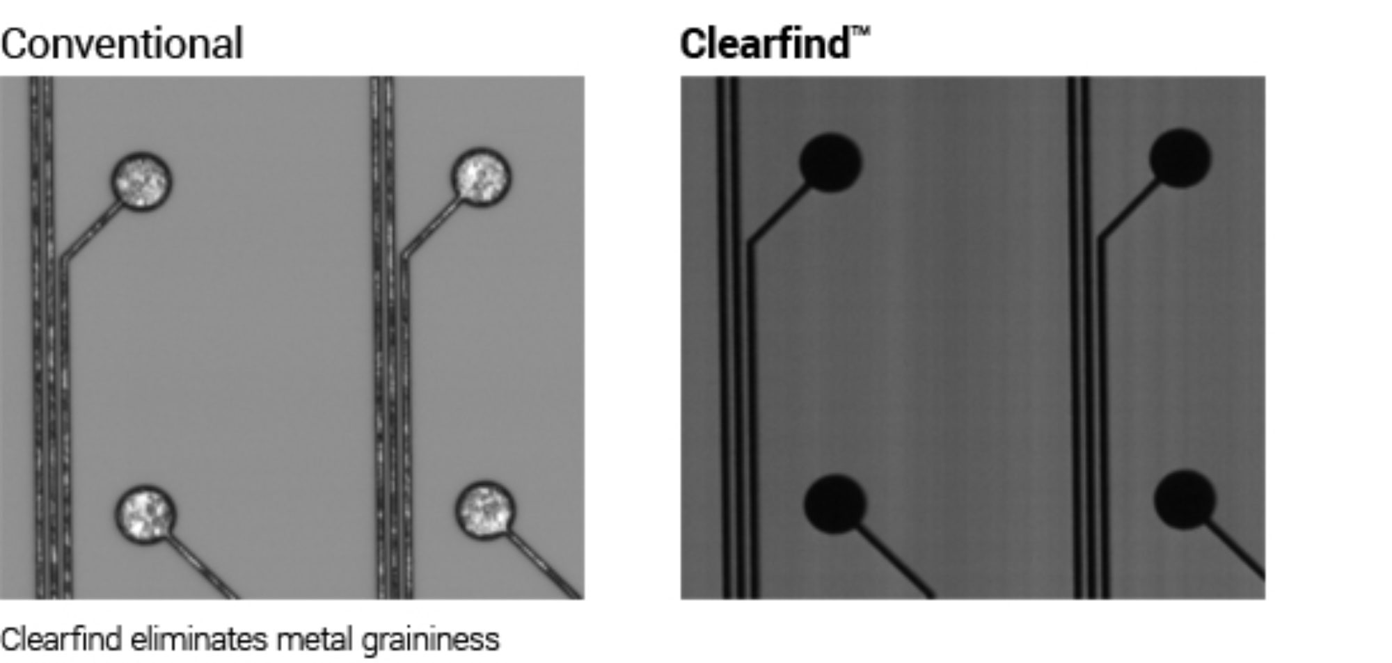
The smartphone and tablet industry has driven thinner and smaller packages which, in turn, drove the rapid adoption of fine pitch interconnect technologies such as copper pillar bumping. While Cu pillar bump diameter and height have been shrinking, an even finer pitch and width requirement is that of the redistribution layer (RDL). The inspection system can be equipped with multiple objectives that allow it to address current packaging applications with 5-10µm RDL L/S and new process development and early productization with future packaging applications with 2µm RDL L/S. Typically, RDL defects of interest are half the size of the RDL width i.e. 1µm for 2µm RDL. But in many cases, the acceptable metal graininess could be larger than the detection size. This leads to a high nuisance rate impacting the total throughput of the wafer, including manual review.
Clearfind® technology can eliminate nuisance defects. The captured images below show the reflected brightlight and Clearfind technology images respectively, for a dense RDL application. In the white light image, it is difficult to detect the 1µm defect as the metal graininess is large and will lead to nuisance defects. This issue is eliminated with Clearfind technology as RDL open and shorts can be detected easily without finding nuisance defects.

For cost effective deployment, the inspection system can also be integrated with a metrology sensor capable of simultaneous thickness measurement of transparent material and RDL height metrology. Onto Innovation software provides the capability to run a defectivity inspection pass that automatically triggers additional metrology passes that are executed in cascade as a function of the defect count limit. This technique could be potentially used to measure the thickness of the residue defect. The inspection and metrology data is exported to Onto Innovation's Discover software system to analyze electrical, metrology and defect data in a single source. This enables faster root cause analysis for quicker ramp and time to market.
To increase and maintain high yields, a production process should be continually monitored to rapidly detect, identify and eliminate any source of defects. Organic defects are not visible or have low contrast when inspected using conventional inspection technology. Onto Innovation's inspection system, equipped with Clearfind technology, is able to flag these defects during production to help eliminate field failures. Combining this technology with brightfield and darkfield inspection on a single platform enables semiconductor device manufacturers to develop and implement an inspection plan to support process, material and equipment characterization, and diagnose systematic process integration issues.
Onto Innovation is leading the way with innovative inspection technologies. Connect with one of our representatives to learn more.