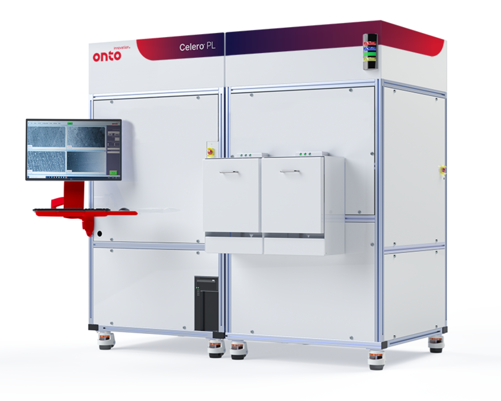
Product Overview
The Celero PL system utilizes a laser-based phase detection and imaging capability that leverages custom optics and image processing algorithms to enable best in class throughput and sensitivity on a broad range of materials and wafer sizes in the rapidly growing compound semiconductor market. Leveraging multiple light sources and sensor channels, the system can detect, measure and image a broad variety of subsurface crystalline defects, associated with bulk wafers and epitaxial layers, surface particles, scratches, pits, surface contamination, stains, point or bulk wafer stress, voids/inclusions, including chips and cracks at the edge of the wafer.
Applications
- Frontside / backside / edge / subsurface defectivity and contamination
- AR/VR/MR materials and structures
- Crystalline defectivity in silicon carbide (SiC) substrates and epitaxial layers
- Crystalline defectivity in gallium nitride (GaN) wafers and epitaxial layers
- Thick wafer / seed wafer surface and sub-surface defectivity
- Substrate-to-epitaxial layer defect mapping (sub-defect mapping)
- Wafer based microLED / VCSEL / EE laser materials
- Across wafer and point stress mapping
- Wafer chuck contamination
- Haze detection and metrology
- Bow / warped wafer metrology
- Thinned wafer inspection (incl. film frame handling)
Specifications
- Wafer sizes: 100 - 300 mm
- Five detection channels: photoluminescence, polarization, slope, bright field and dark field
- All-surface scan (FS/BS/Edge) and imaging with sub-nanometer sensitivity
- Particle defect (≥90nm PSL) / surface contamination (≥5Å)
- Thin (≥100µm) and thick (≤10mm) wafer
- Multiple handling options: wafer, film frame
- Multiple load options: manual, automated open cassette, EFEM
- Online and offline review capability
- Automated Image Based Defect Classification
- Compatible with Discover® ecosystem