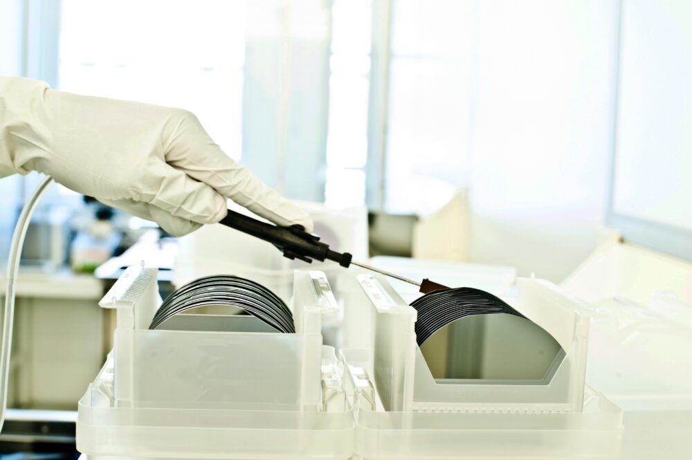
Controlling impurities in Silicon and monitoring Epi thickness and variation is the basis for improved performance of devices in the world’s electronics industry.
Measurement of Interstitial oxygen and substitutional carbon content in silicon is an important material characteristic for most modern device technologies. These measurements start at the ingot level or on thicker slugs or on thinner product wafers. Transmission based FTIR/FRS technology is used to efficiently generate oxygen profiles along the whole rod or crystal or wafers. This technique provides the wafer suppliers with rapid feedback for continuous process improvement and control. Accurate calibration to NIST certified standards and routine use of the FTIR technology has been demonstrated with minimal interference from radial oxygen gradient and predictable interference from resistivity over a wide range of product specifications.
The epitaxial layer is a thin layer of silicon typically designed to have different compositional and electrical properties from the underlying wafer, tailored to the specific demands of the device. Monitoring the thickness and the uniformity of this layer provides increased reliability during the fabrication process.
Reflection based FTIR technology is used to monitor epitaxial thickness and uniformity and provides feedback to build the most complex and sophisticated devices in the semiconductor world.


