Article posted on Jan 28, 2018
As electronic devices become ever more pervasive in our daily lives, ensuring their quality and reliability has become not just desirable, but in some cases, a life or death requirement—consider the possible consequences of a catastrophic failure in a medical device or the control system of an autonomous car. Electronics manufacturers are under growing pressure to build quality and reliability into their devices and that pressure is magnified by the increasing criticality of the applications. Although this is not a new demand, it is made more challenging by the appearance of new process and packaging technologies that pack greater functionality into less space through vertical integration. All of these technologies require connections in the third dimension, above or below the die, thus adding, quite literally, a new dimension to inspection and metrology requirements.
Consumer tolerance for device failure is at an all-time low, as they demand more functionality and more convenience from their electronic devices. The results of failure range from minor inconvenience – a wait in a long line because a dead cell phone could not retrieve a boarding pass – to catastrophe from a failed pacemaker or wrecked car. The automotive industry is an excellent example. Its relentless focus on reliability is driven not only by the cost of failure in human terms, but also by market forces such as costly recall and foreign competition implications. When cars contained only a few electronic components, a failure rate of one in a million might have been acceptable. Autonomous cars may each have tens of thousands of electronic components, making one-in-a million not nearly good enough.
The microelectronics industry has followed a familiar narrative since its birth—put more computing power and functionality in less space; only now it has entered, quite literally, a new dimension—vertical.
Packaging these vertically-integrated die requires the need to provide interlayer connections that are as small and reliable as the multilayer interconnect technologies used within the chip. This need for vertical connections has created a whole new class of technologies – advanced packaging – with a whole new lexicon of terms (and acronyms): through-silicon vias (TSVs), redistribution layers (RDLs), bumps, pillars, nails, under bump metallization (UBM), wafer-level packaging (WFP), fan-in, fan-out and many more. All these technologies serve the purpose of providing reliable, electrically isolated, vertical connections, and most, at some point, involve the creation of a conductive “bump” protruding through an insulating layer to carry the signal to the next layer above or below.
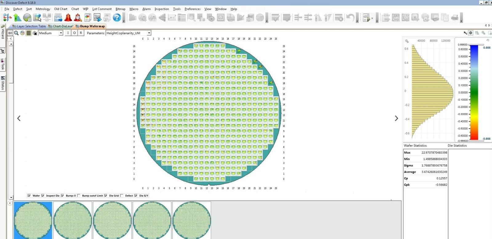
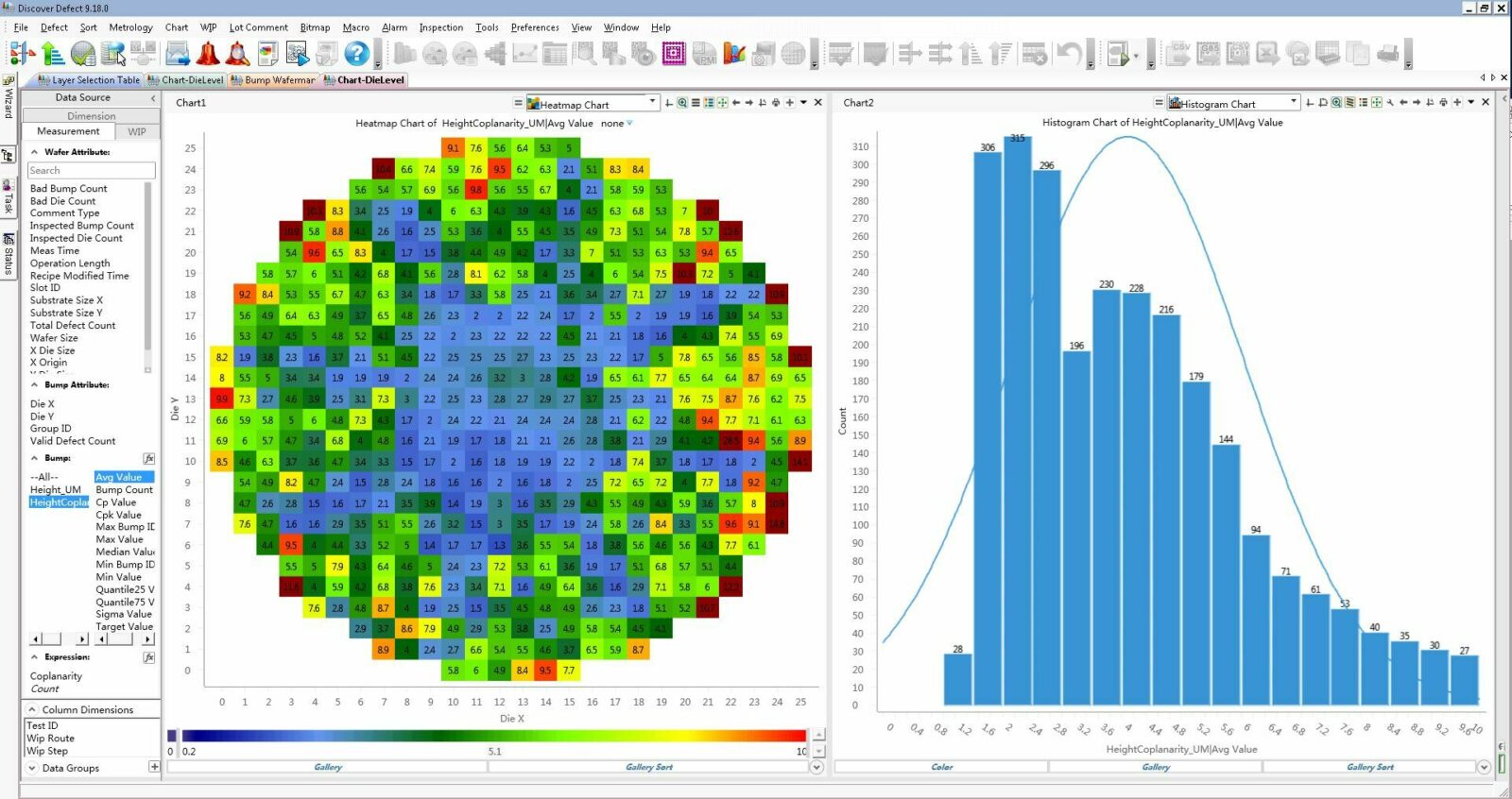
As these bumps have become smaller and denser, fabricating them reliably has required the adoption of process control technologies, including extensive inspection and metrology. Total bump process control refers collectively to the 2D/3D inspection and metrology requirements of this class of technologies. Controlling these processes is critical to ensuring the reliability of the finished device and requires the combination of standard 2D techniques with a new class of 3D technologies. As dimensions shrink, repeatability and resolution requirements will increase, surpassing the capability of white light techniques and requiring the use of laser-based technologies. But total bump process control requires more than just new sensors, it requires a comprehensive approach advanced analytics—distilling classified, usable results from the torrent of raw data created by these new technologies. As shown in Figure 1, software to visualize bump coplanarity gives users a powerful tool to quickly assess various bump heights within a set tolerance. In addition, inspection and metrology systems must have the flexibility to control all kinds of bumping-related processes: wafer-level chip-scale packaging (WLCSP), ball drop, micro-solder, Cu pillar, RDL height, UBM height and more.