Product Overview
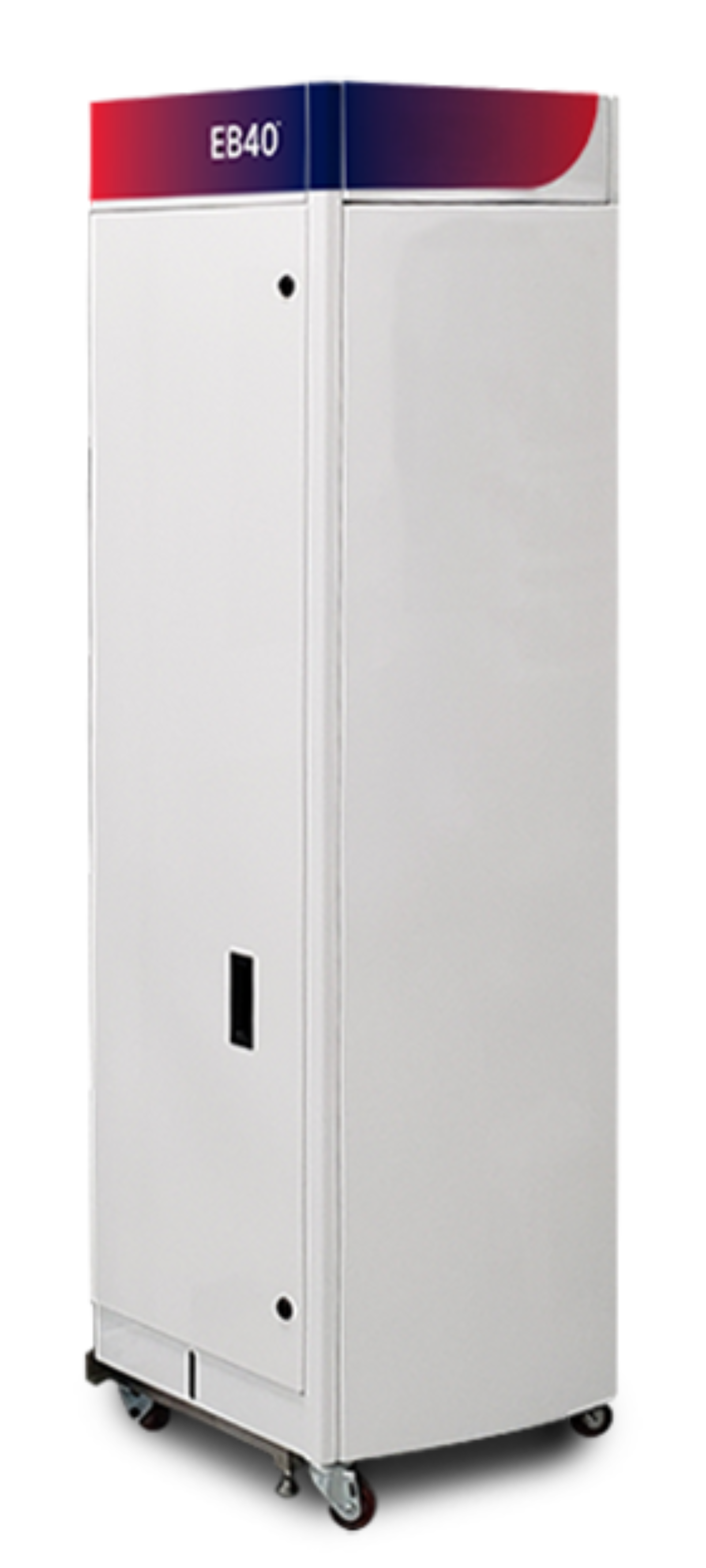
The Class 1 certified E40 and B40 modules (available separately or combined in one module) can automatically detect defects on the entire edge, from zone 1 to 5, and the entire backside. The ability to inspect the entire backside allows for faster root-cause analysis of zone 5 defects since such defects can migrate from the wafer interior.
The EB40 module captures defect images on the fly, creates whole-wafer composite images, and is fully integrated for SEM bevel review. All inspection and metrology results, including defect, whole wafer and SEM images can be analyzed together in a single database using our Discover Defect software analysis package. Correlating EBR metrology with all-surface defectivity data, SEM data and micro-inspection results is only the beginning of what Discover software can do. In addition to the advanced on-tool defect binning, real-time edge ADC classification can be assigned to defects prior to manual offline review using Discover Review software.

Applications
Edge Inspection
- Lithography process monitoring
- Cracks/Chips
- Residue
- EBR Concentricity
- Bonding adhesive inspection
Backside Inspection
- Scratches
- Chuck/end effector signatures
- Wafer level pattern detection
- Backside defect to frontside defect correlation
Specifications
- Detects blister defects
- Detects slurry, cleaning contaminants and residual films
- Automated Edge Bead Removal metrology (EBR)
- Detects chips and cracks
- Addresses contamination issues
- Finds delamination defects
- Backside particles and residues
- Wafer level defect signatures
- Detects scratches and defect clusters