Imaging of Overlay and Alignment Markers Under Opaque Layers Using Picosecond Laser Acoustic Measurements

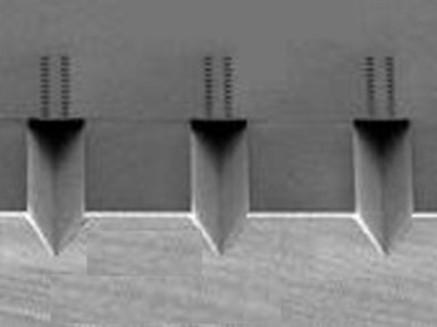
Optically opaque materials present a series of challenges for alignment and overlay in the semi-damascene process flow or after the processing of the magnetic tunnel junction (MTJ) of a Magnetic Random-Access Memory (MRAM). The overlay and alignment of a lithographically defined pattern on top of the pattern and the underlying layer is fundamental to device operation in all multi-layer patterned process flows. There are a wide variety of optical techniques and specially designed targets (Figure 2) that are used to address this problem in conventional flows. Typically, either an ultraviolet, visible, or infrared light is coupled through the top photoresist layer or an etched hard mask to be aligned to the bottom layer [1]. However, in some MRAM flows this coupling may not be possible as there may be an intervening opaque layer (Figure 1). In such cases, conventional methods of alignment using light fail. To overcome this issue, extra patterning operations may be used to open areas around the alignment features, but these operations add significant process cost.
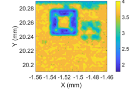
In this paper we evaluate the use of picosecond laser acoustics (PLA) measurement as an alternative method to characterize the overlay and alignment patterns that are embedded under opaque metal films. We selected the MRAM process flow for this study where the different overlay and alignment markers were underneath opaque layers including an MTJ layer. These specific markers are imaged with the help of PLA employing an ultrafast laser in a pump and probe configuration to generate and detect acoustic waves capable of propagating through optically opaque layers. This technique, in sharp contrast with other competing acoustic imaging techniques such as scanning acoustic microscopy (SAM) [5,6], does not require the sample to be submerged in a coupling medium such as water.

