Onto Innovation Defect Inspection Products
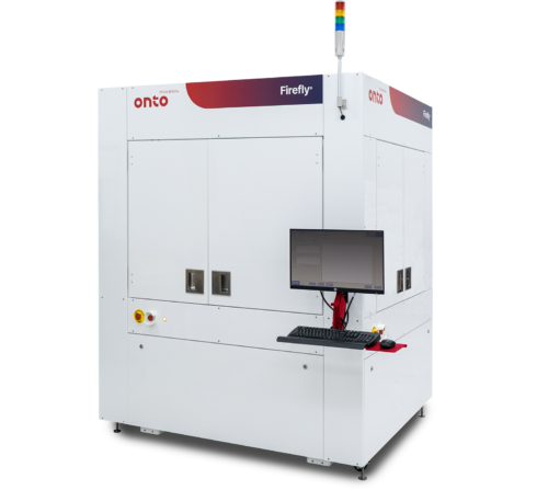
Firefly G3 System
Sub-micron automatic defect inspection for advanced IC substrates and panel level packaging
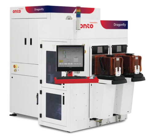
Dragonfly G3 System
Automated high speed sub-micron 2D inspection and combo 3D inspection/metrology for inline process control of pattern defects and next generation technologies for advanced packaging, specialty and OQA
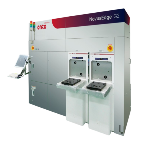
NovusEdge G2 System
Unpatterned edge, notch and backside inspection
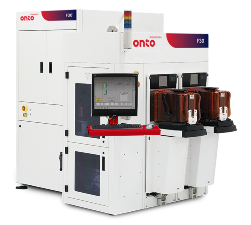
F30 System
Advanced macro inspection for front-end manufacturers
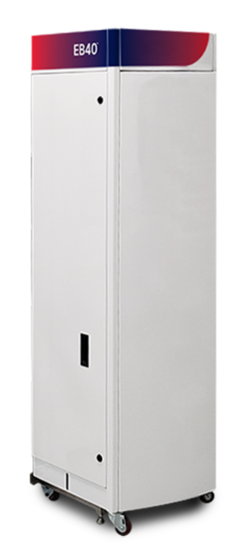
EB40 Module
Edge and backside inspection
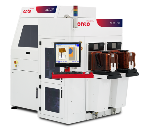
NSX 330 System
2D automated defect inspection and sample 3D inspection for advanced packaging
Inspection Tool Productivity Software
Software solutions to increase the value of data available from your inspection tool
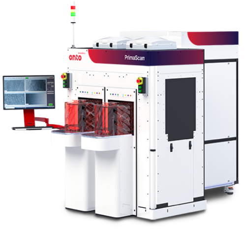
PrimaScan Series
All-surface contamination and defectivity inspection and imaging capability for both opaque, transparent and semi-transparent wafers, reticles and glass panel level substrates
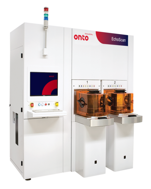
EchoScan System
Opto-acoustic void detection in buried layers and bonded wafers