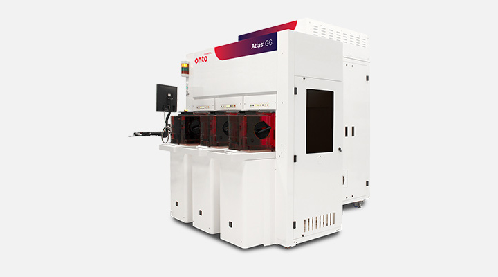
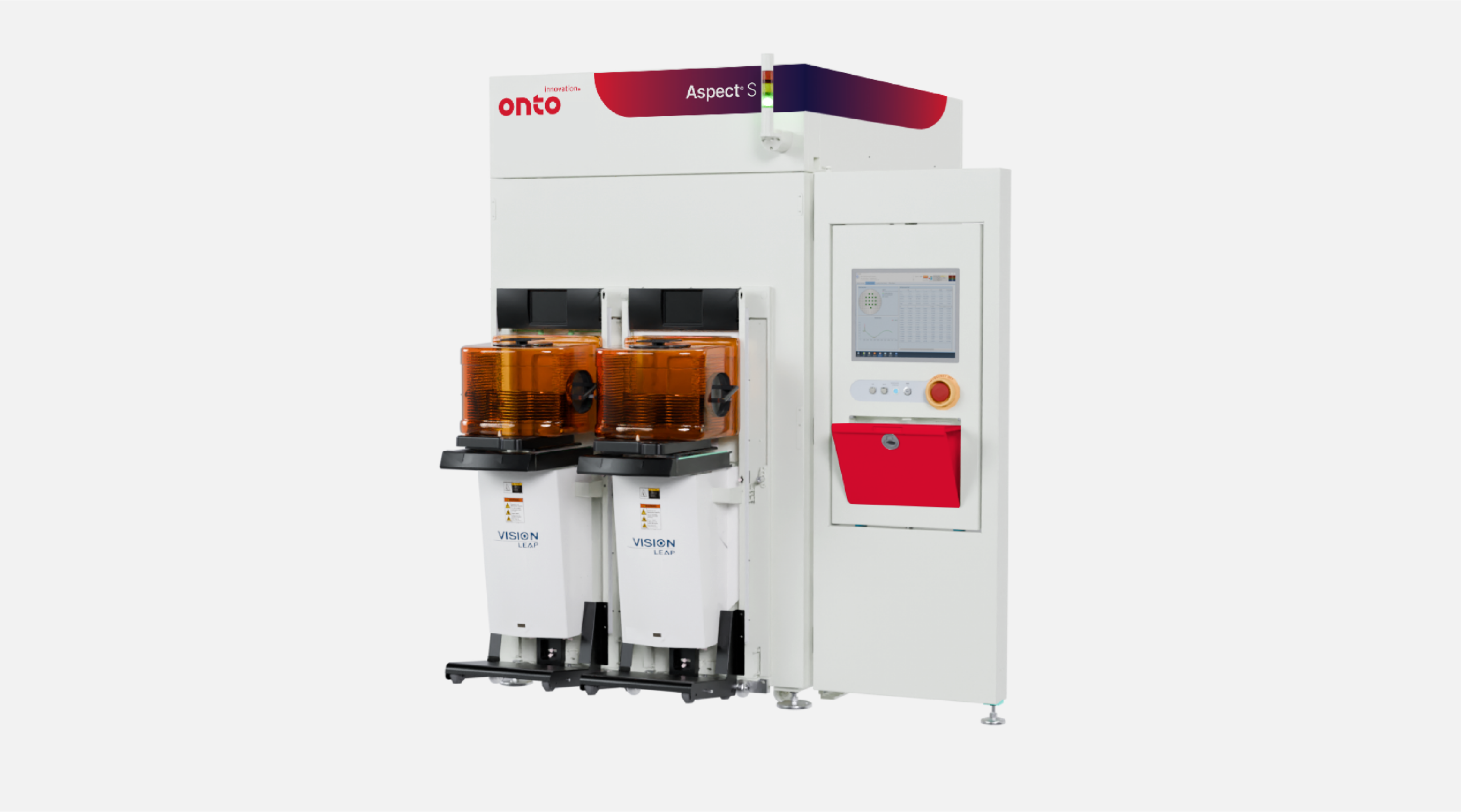
Metrology
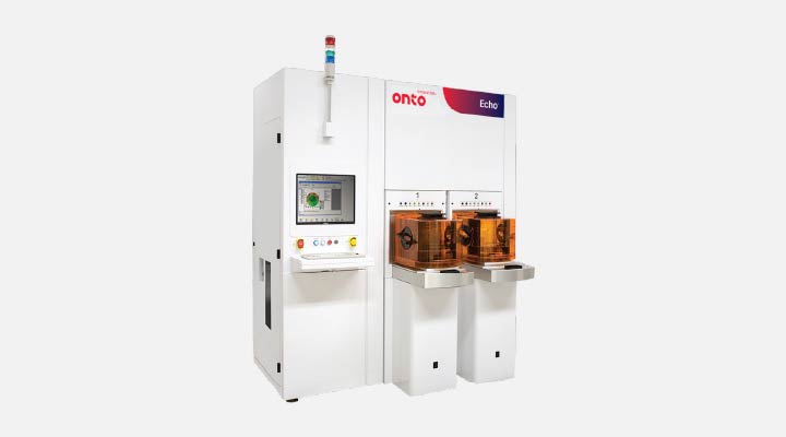
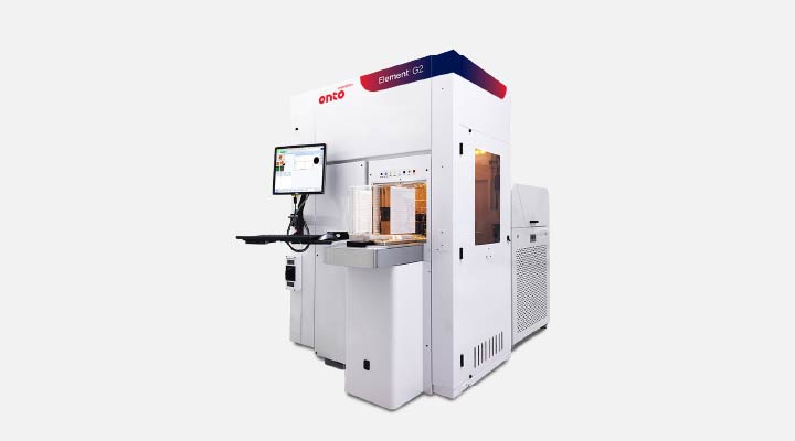
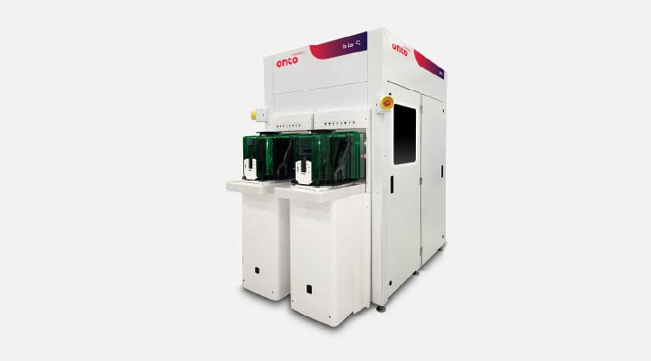
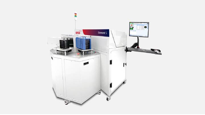
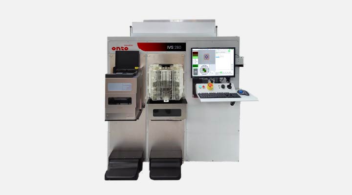
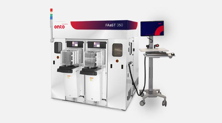
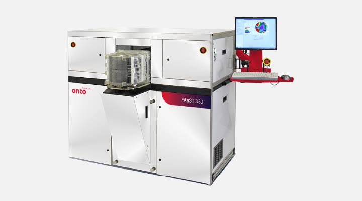
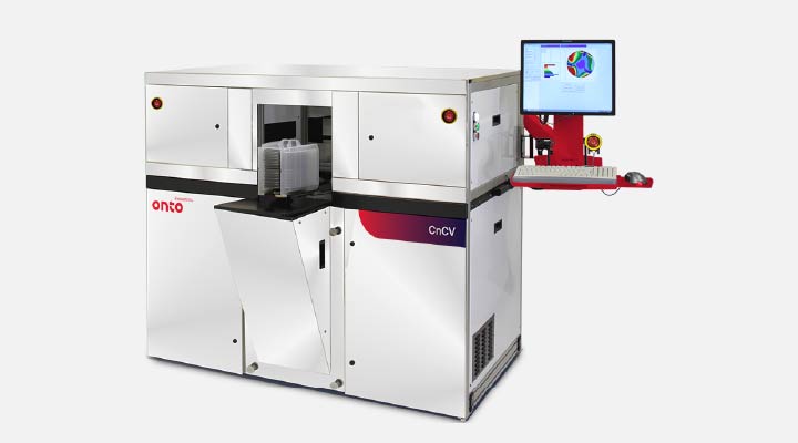
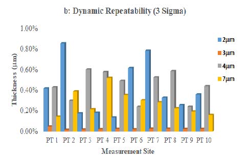
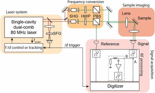
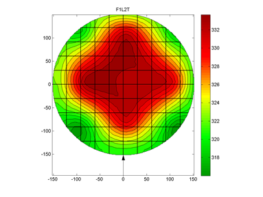
Advanced optical critical dimension (OCD) and film metrology products to help ensure accuracy and repeatability for semiconductor manufacturers worldwide
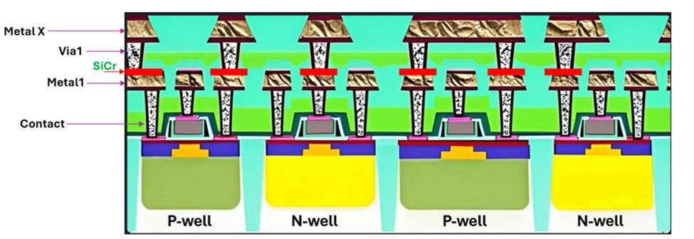
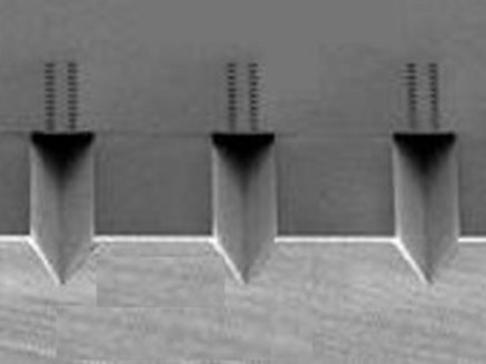
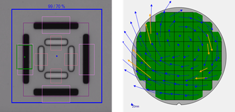
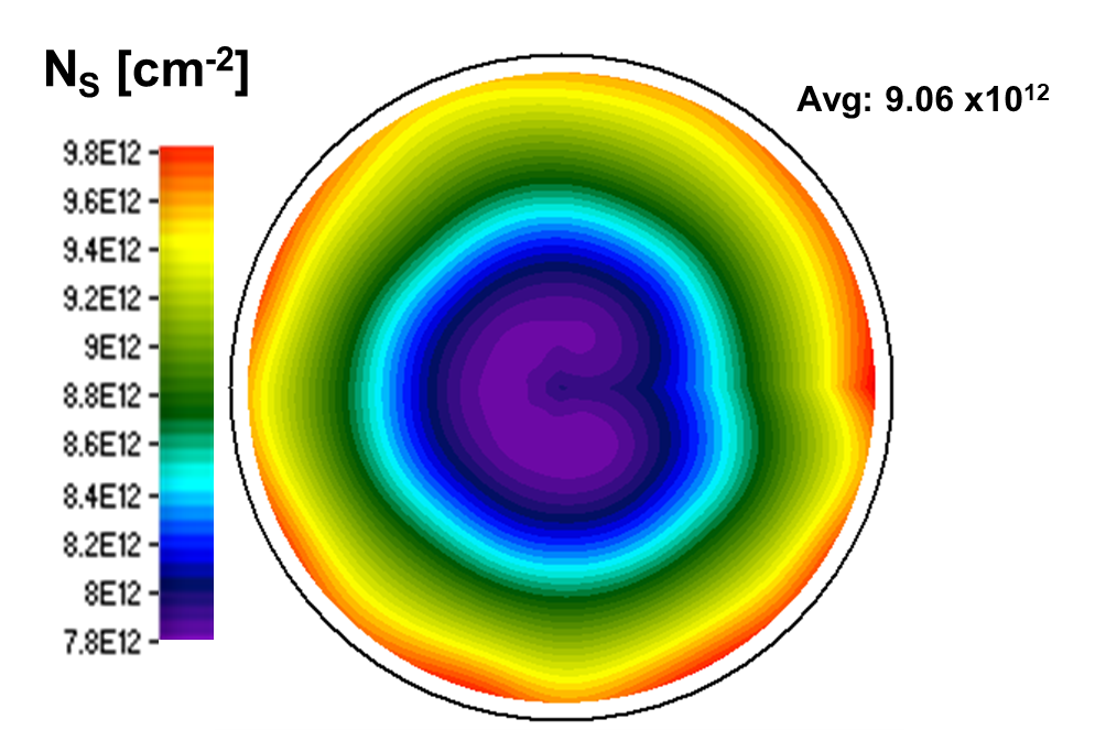
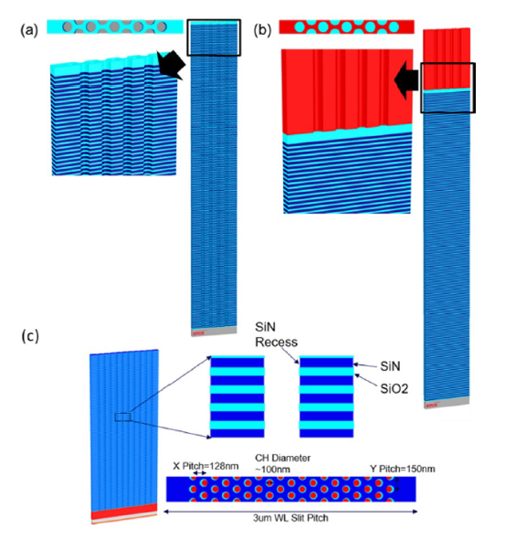
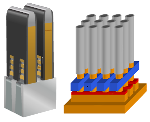
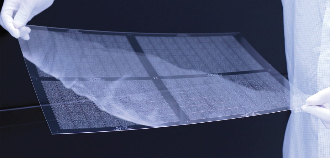
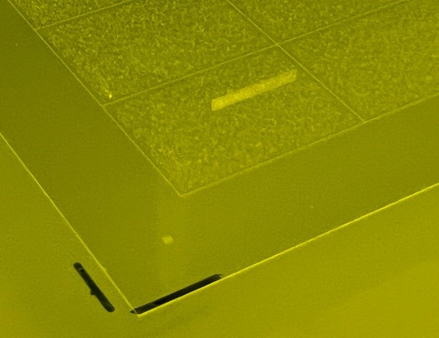
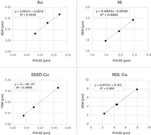
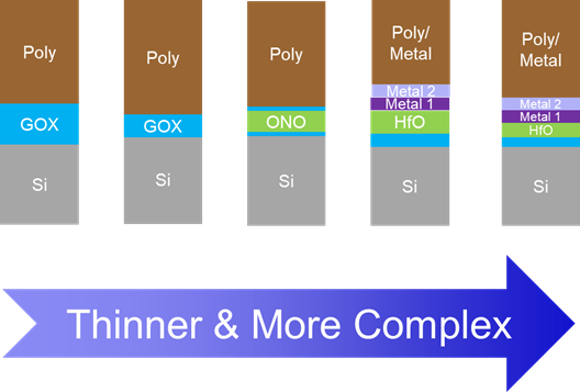
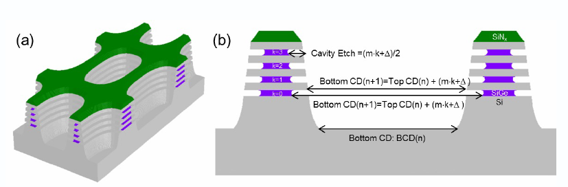
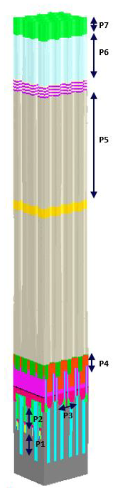
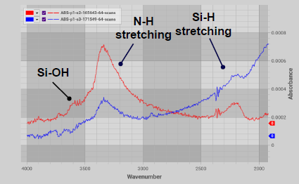
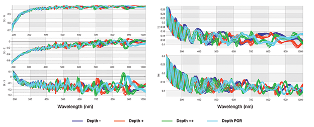
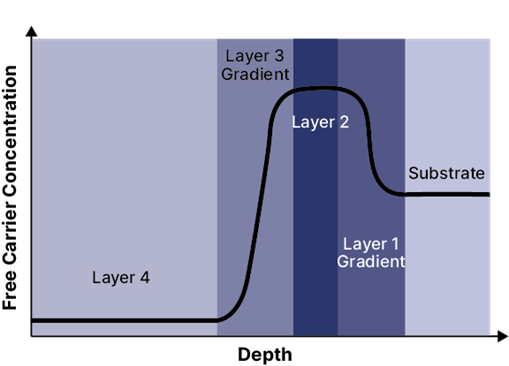
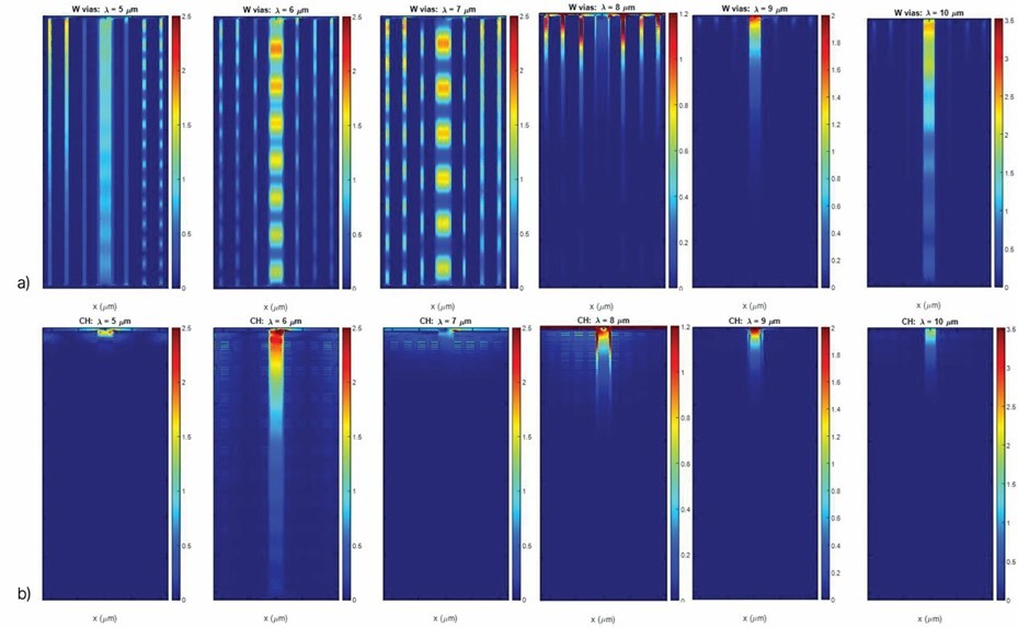
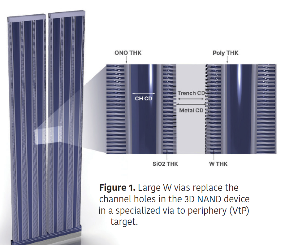
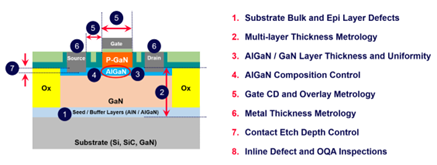
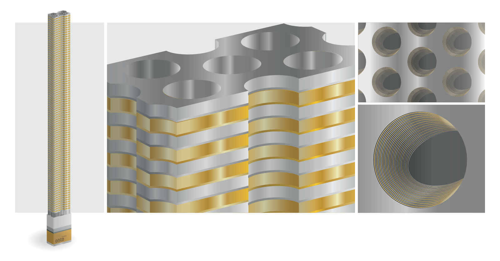
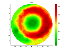
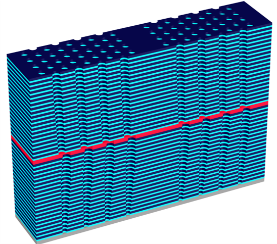
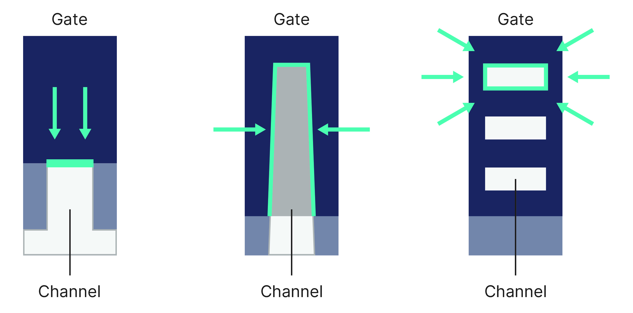
As semiconductor chips become increasingly complex, the demand for precision dimensional and films metrology intensifies.
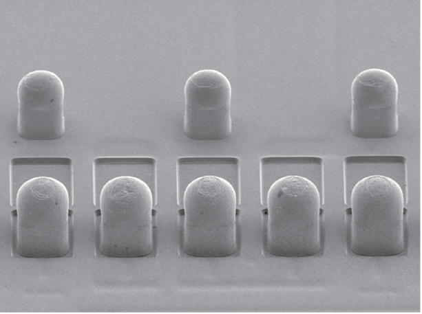
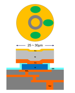
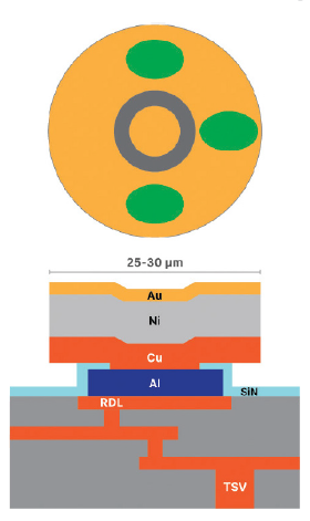
Traditionally vital for semiconductor logic and memory markets, advanced metrology is seeing expanded adoption in next-generation advanced packaging technologies and specialty applications as these segments continue to grow in value and become increasingly sophisticated.
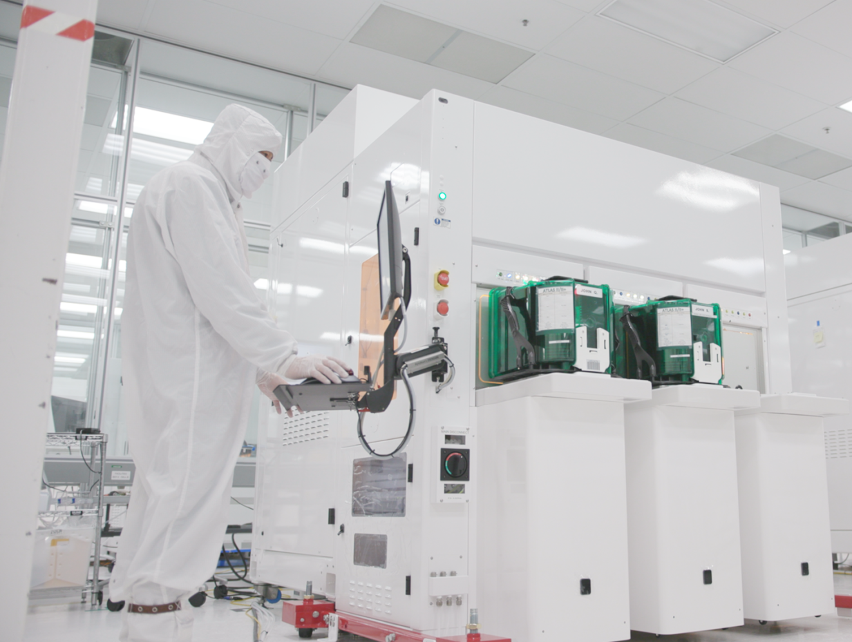
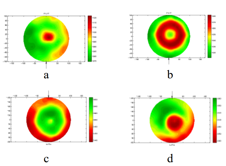
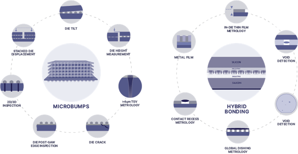
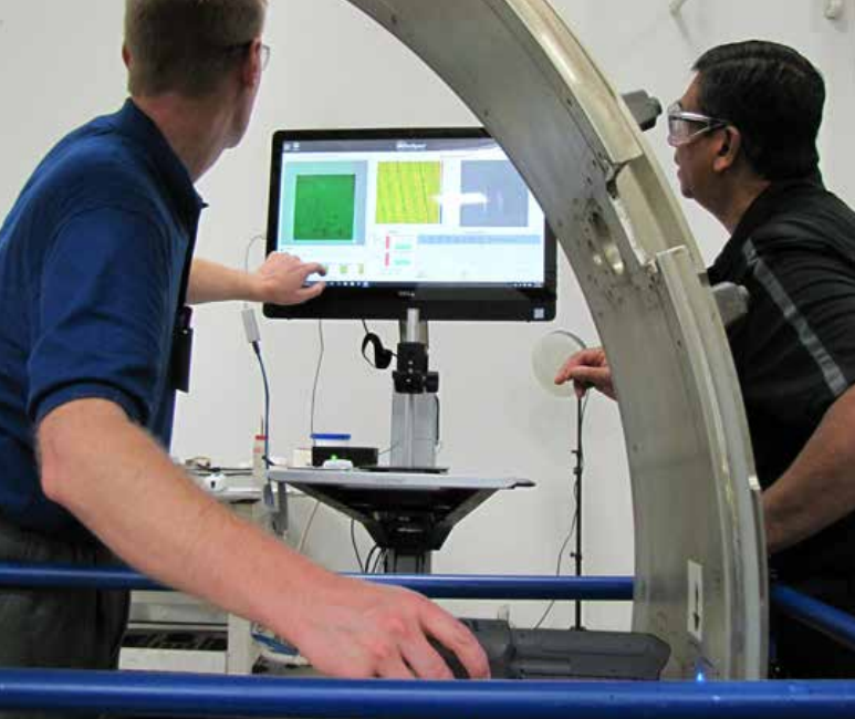
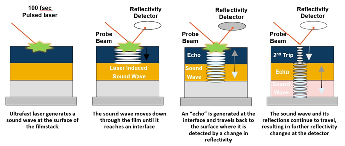
Our comprehensive metrology solutions include OCD, films, overlay and composition metrology. These tools are crucial for detecting process excursions in high volume manufacturing and are instrumental in R&D for helping to develop the newest devices. We offer integrated and inline metrology solutions, powered by Onto Innovation’s AI-guided modeling and analysis software, to ensure high accuracy in-line optical metrology and efficient offline recipe development.
Iris™ G2 System
IMPULSE® V System
IVS 380 System
Atlas® V System
Echo™ System
Element™ G2 System
Aspect® System
Iris™ S System
Element™ S System
IVS 280 System
OCD Solutions
IMPULSE®+ System
Atlas® III+ System
Through the Glass: Why the Rapid Development of TGV Demands Rigorous Analysis
Interconnect Innovations in High Bandwidth Memory, Part 1
Enhancing CMP Process Control with Intelligent Line Monitoring & Integrated Metrology
Bridging Performance and Yield: The Evolving Role of Interconnect Technologies in HBM
Comprehensive Process Control Solutions for Through Glass Vias
Enabling In-Line Process Control for Hybrid Bonding Applications
Using Picosecond Ultrasonic Technology for AI Packages, Part 2
Front-End Technologies Are The New Back-End Tools: Using Picosecond Ultrasonics Technology For AI Packages, Part 1
CD Step Application in Edge Air Layer Structure Measurement for Bulk Acoustic Resonator
Picosecond Ultrasonics: An Advanced Technology Utilized for Process Control of SiCr Thin Film Resistors
Advanced Interconnect Process Control with Picosecond Ultrasonic Technology for AI Device Packaging
Applications of Picosecond Laser Acoustics for Advanced Packaging
Measuring Multi-Layer Ultra-Thin Critical Films
Optical Critical Dimension Metrology with Spectroscopic Ellipsometry
Addressing The Challenges of Metrology for Advanced Packaging
Using 2D/3D Technology to Overcome Challenges of Large-Area Panel Inspection and Metrology
Using Picosecond Ultrasonics To Measure Trench Structures In SiC Power Devices
Non-destructive Measurement of Bottom Width in Deep Trench Isolation Structures Using IRCD Metrology
Non-destructive Metrology Techniques for Measuring Hole Profile in DRAM Storage Node
Advanced FTIR Optical Modeling for Hydrogen Content Measurements in 3D NAND Cell Nitride and Amorphous Carbon Hard Mask
Using OCD To Measure Trench Structures in SiC Power Devices
Using FTIR To Improve SiC Power Device Performance
Changing Shop Floor Metrology From a Cost to a Benefit
The Road to SiC Process Control
Optimizing Metal Film Measurement on IGBT And MOSFET Power Devices with Picosecond Ultrasonic Technology
3D NAND Needs 3D Metrology
Measuring the Critical W-recess in 3D NAND
The Age of Hybrid Bonding: Where We Are and Where We’re Going
A Star is Born: Gallium nitride and the coming age of compound semiconductors
Efficient pump-probe sampling with a single-cavity dual-comb laser: Application in ultrafast photoacoustics
Metrology Sampling Plans Are Key For Device Analytics And Traceability
Paving the Way for 5G: RF Filter Process Monitoring and Control Using Picosecond Ultrasonic Metrology
Critical Moves: Advanced Logic Devices And CIS Benefit From Applications Using IRCD Metrology
Advanced Modeling In FTIR Offers New Applications For HVM
Optical Critical Dimension Metrology for Semiconductor Manufacturing
Reducing Rework In CMP: An Enhanced Machine Learning-Based Hybrid Metrology Approach
Expanded Material Metrology For Refined Etch Selectivities
Imaging of Overlay and Alignment Markers Under Opaque Layers Using Picosecond Laser Acoustic Measurements
Mid-Infrared Optical Metrology for High Aspect Ratio Holes in 3D NAND Memory Manufacturing
Advantages of Picosecond Ultrasonic Technology for Advanced RF Metrology
Untangling 3D NAND: Tilt, Registration, and Misalignment
Metrology Solutions for Gate-All-Around Transistors in High Volume Manufacturing
Monitoring Critical Process Steps in 3D NAND using Picosecond Ultrasonic Metrology with both Thickness and Sound Velocity Capabilities
Full Metrology Solutions for Advanced RF with Picosecond Ultrasonic Metrology
Artificial Intelligence and Machine Learning in Semiconductor Manufacturing: Inspection and Metrology
Do you have a metrology question? Let’s talk!
As your partner for innovative solutions, we’re always here for you.
Discover how our cutting-edge semiconductor solutions are engineered to meet your most complex challenges: delivering performance, reliability and innovation where it matters most.
Let’s Talk
"*" indicates required fields