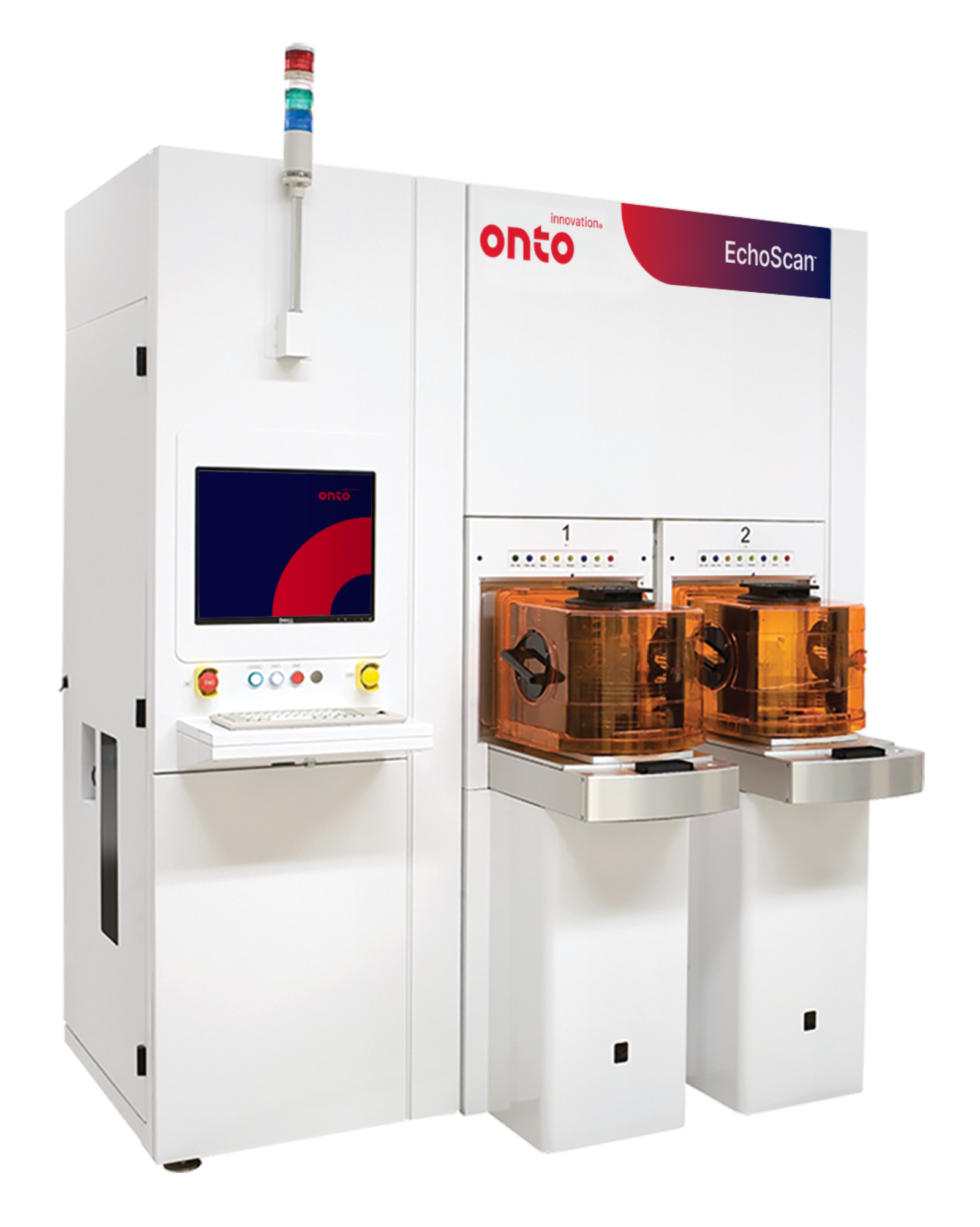
Product Overview
The EchoScan system is a die and wafer-level immersion-free non-contact technology to detect voids down to 1µm sensitivity in high volume manufacturing. Based on proprietary PULSE technology, Onto's solution uses properties of laser/matter interaction to detect voids whether they are located in dielectric or metal layers. This unique IR wavelength laser-based system enables detection through full Si thickness and can image voids in buried structures and/or bonded interfaces.
When paired with Discover analytical software, the EchoScan system enables real-time defect analysis and feedback to process tools for statistical process control, reducing the cycle time of yield loss assessment and helping customers achieve high volume manufacturing goals.

Applications
- Void detection in direct bonded and hybrid bonded wafers
Related Products & Markets
Echo System
Opto-acoustic film metrology for in-line metal film thickness measurements and material characterization.
Memory
Acoustic film metrology system that provides accurate, in-line thickness measurements of semi-transparent and metal films on product wafers
Logic/Foundry
Acoustic film metrology system that provides accurate, in-line thickness measurements of semi-transparent and metal films on product wafers