Series Overview
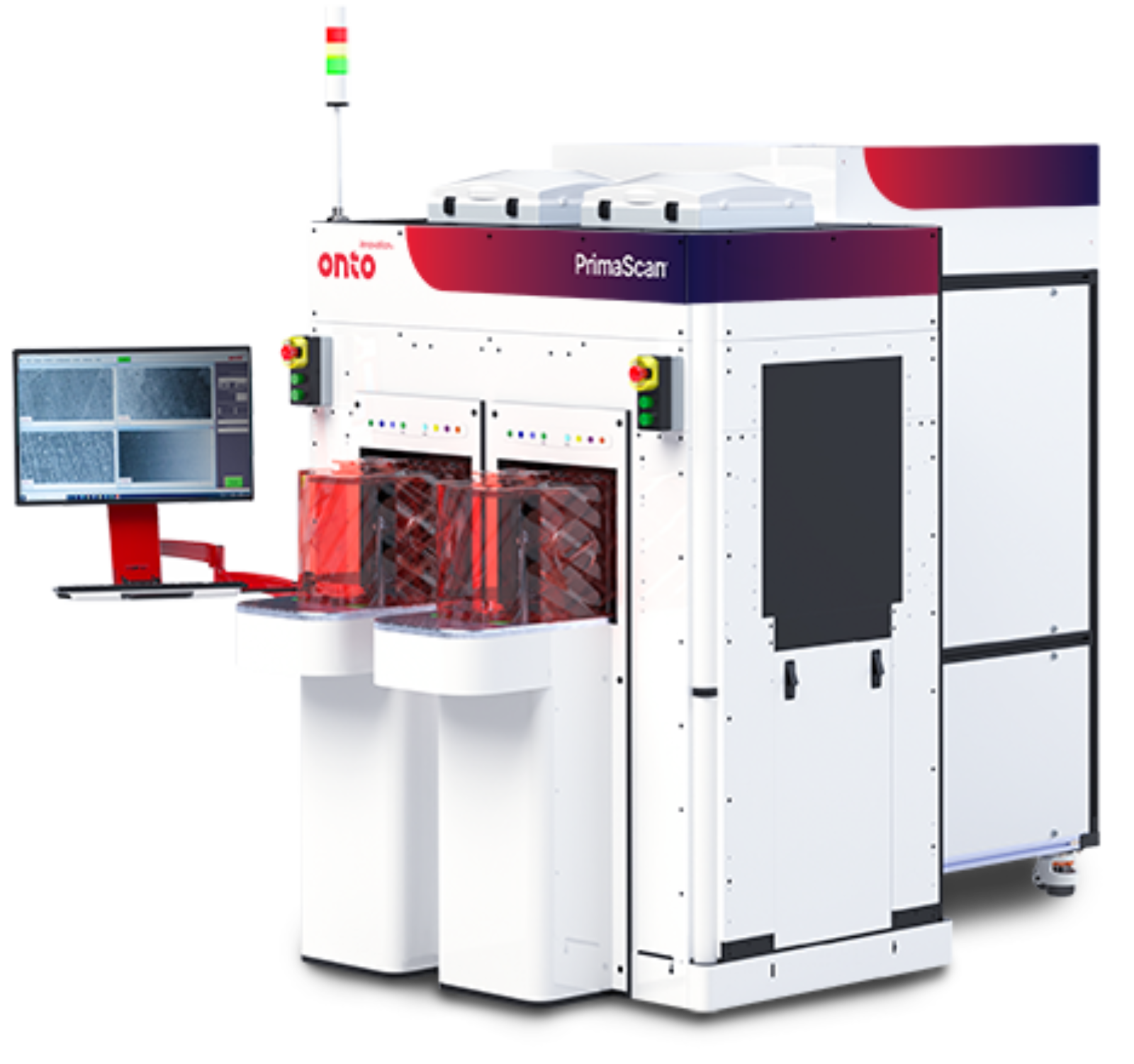
PrimaScan System
The PrimaScan system delivers a unique laser-based scanning and imaging technique leveraging proprietary optics and sensing technologies for reliable inspection of nanometer sized defects on a variety of opaque and transparent/semi-transparent substrates suitable for either R&D or high-volume manufacturing environments. Utilizing multiple channel inspection technologies, the system can detect, measure and image surface particles, scratches, pits, surface contamination, stains, film or bulk wafer stress, voids/inclusions, including chips and cracks at the edge of the wafer.
The PrimaScan product line is suitable to address challenges in both incoming wafer quality control and in inline process monitoring. Leveraging its ability to handle a wide variety of substrate materials, it uniquely addresses process monitoring and control challenges in the production of silicon carbide (SiC) based devices, glass based microfluidics and AR/VR/MR related applications on a variety of transparent and semi-transparent materials.
Designed with versatility in mind the PrimaScan line of wafer-based inspection tools can handle a variety of wafer sizes and substrate types including film frame, photomask and sample tray.
Applications
- Opaque, transparent or semi-transparent bulk wafers
- Dielectric or metallic coated wafers
- Coating thickness variation for glass in microfluidics
- Monolayer organic residues
- Wafer chuck contamination
- Internal stress, air gap, glue overflow for microlens arrays for AR/VR/MR (including CIS)
- Voids in transparent: films, wafers and bonded wafers
- Flat optics contamination
- Glass wafer edge chip
- Haze detection and metrology
- High bow / warp wafer handling and measurement
- Incoming wafer quality
- Photoresist coating defects
- Photomask blank
- Post-grind / taiko wafer (or film frame) defectivity
- Gel and waffle pack inspection
- JDEC sample tray sample inspection
Specifications
- Wafer Sizes: 100 - 450mm
- Four detection channels: polarization, slope, bright field and dark field
- All-surface scan (frontside/backside/edge) and imaging with sub-nanometer sensitivity
- Particle defect (≥90nm PSL) / surface contamination (≥5Å)
- Simultaneous frontside / backside inspection (transparent & semi-transparent substrates ONLY)
- Thin (≥100µm) and thick (≤7mm) wafer / substrate handling
- Multiple handling options: wafer, photomask, film frame, JDEC tray, waffle pack
- Multiple load options: manual, automated open cassette, EFEM
- Automated Image Based Defect Classification
- Online and offline review capability
PrimaScan P System
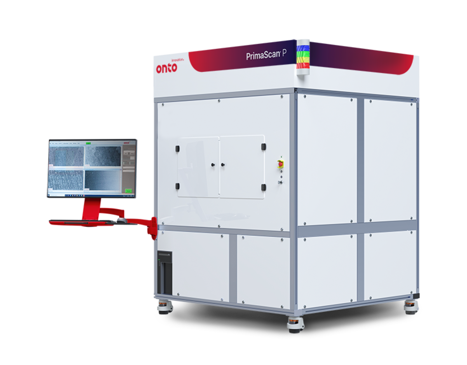
As the panel substrate segment of the advanced packaging market transitions to from copper-clad laminates (CCL) to glass the industry must adapt its substrate monitoring discipline to ensure starting substrates are free of killer defects or latent defects that may result in yield loss or scrapped panels at later stages in the process flow. The PrimaScan P system is specifically designed to address challenges in incoming glass panel quality control for both the advanced IC substrate (AICS) and fan-out panel level processing (FOPLP) application segments within the rapidly growing advanced packaging market.
The PrimaScan P system is enabled by a unique laser-based scanning and imaging technique leveraging proprietary optics and sensing technologies for reliable inspection of nanometer sized defects on a variety of glass substrate sizes and is suitable for either R&D or high-volume manufacturing environments. Utilizing multiple channel inspection technologies, the system can detect, measure and image surface particles, scratches, pits, surface contamination, stains, film or bulk panel stress, voids/inclusions, including chips and cracks at the edge of the panel.
Applications
- Incoming unpatterned glass panel quality inspection
- Blanket dielectric or metallic coated panels
- Coating thickness variation for glass
- Monolayer organic residues
- Photoresist coating defects
- Across panel stress and induced point stress
- Voids in transparent films
- Glass panel wafer edge chip
- Haze detection and metrology
- High bow / warp panel handling and measurement
Specifications
- Panel sizes: ≤ 600mm x 600mm
- Four detection channels: polarization, slope, bright field and dark field
- All-surface scan (frontside/backside/edge) and imaging with sub-nanometer sensitivity
- Particle defect ≥150nm PSL / surface contamination ≥5Å
- Simultaneous frontside / backside inspection (transparent & semi-transparent substrates ONLY)
- Thin (≥100µm) and thick (≤5mm) panel handling
- Multiple load options: manual, EFEM
- Automated Image Based Defect Classification
- Online and offline review capability