

Onto makes possible the world of tomorrow through
The Power of
Connected Thinking
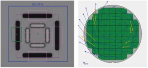
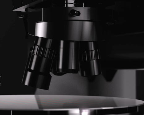
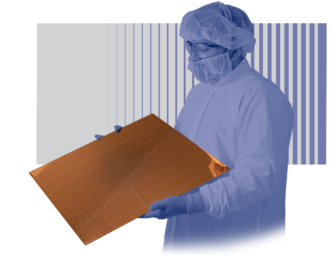
Onto Innovation provides comprehensive process solutions across the semiconductor value chain, specializing in inspection, metrology, lithography and software. Solving our customers’ most complex challenges, enabling a more innovative future.

Featured News
Onto Innovation to Report Second Quarter 2026 Financial Results on August 6, 2026
Article
Unlocking Scalable SRG Waveguides for Mass‑Market AR/MR Displays

Event
SEMICON Taiwan

Contact
Do you have a challenge? Discuss with our Team.
Set apart by innovation


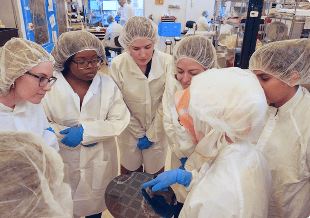
Join our future focused team today
Are you a passionate innovator ready to help shape the future of what technology can achieve? Join us at the forefront of semiconductor innovation, where your ideas can power the world of tomorrow.