Picking up the Pace of Panel-level Advanced Packaging at Onto Innovation
The Era of AI, coupled with the emergence of glass substrates, is set to accelerate the need for panel-level advanced packaging technologies. As AI chipsets increase in size, moving to panel format makes sense to increase yield and reduce waste. It’s the basic square-peg/round hole dilemma.
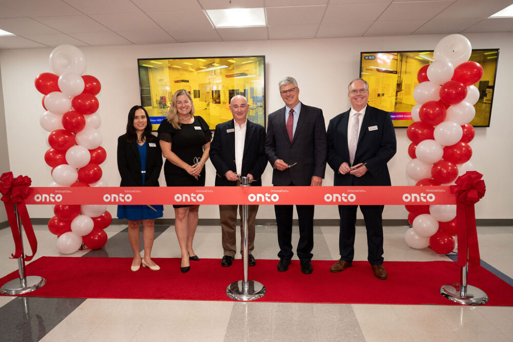
On September 30, 2024, 3D InCites' Françoise von Trapp visited Onto Innovation’s headquarters in Wilmington, MA to attend the grand opening of its Packaging Applications Center of Excellence (PACE). The company has partnered with like-minded suppliers of the PLP ecosystem to accelerate the development of PLP technologies for both organic and glass substrates.
