Product Overview
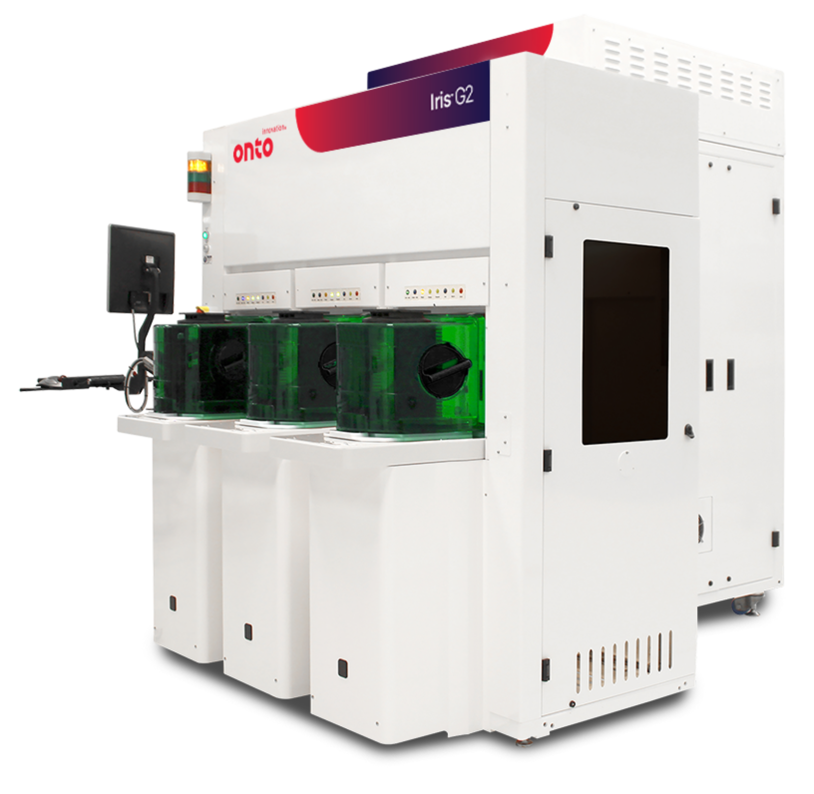
Iris G2 System
Common and Critical Thin Film System
The Iris G2 system is a single platform film metrology system for both common and critical films for advanced node, mature and specialty device applications. As semiconductor device technologies become increasingly complex, requiring thinner and more uniform films, the need for a stable, all-in-one thin film metrology solution becomes a necessity. By controlling the quality and effective thickness of gate films, the Iris G2 system enables advanced logic manufacturers to increase transistor speed, reduce power consumption and improve reliability.
For ultra-thin multilayer films measuring 10Å to 50Å, the Iris G2 system features deep ultraviolet (DUV) spectroscopic ellipsometry (SE) for common films and a coupled proprietary laser ellipsometry technologies for critical films, providing customers with the flexibility to optimize cost of ownership, better stability, and ease of operation in a versatile tool for specialty, mature and advanced logic and memory processes.
Applications
- Critical film measurement
- Gate Oxide
- HiK Metal Gate
- Other single or multi-layer ultra-thin dielectric and semiconductor films
- Wafer bow, warp, and film stress
- Common film measurement
- Photoresist and polymers
- Dielectric films (oxide, nitride, high-K and low-K films)
- Silicon and compound semiconductors (Si, Poly, SiGe, GaN, AlGaN, SiC, etc.) films
- Silicide and metal compound films
- 2D and 3D OCD measurement
Iris System
For 300mm silicon manufacturing
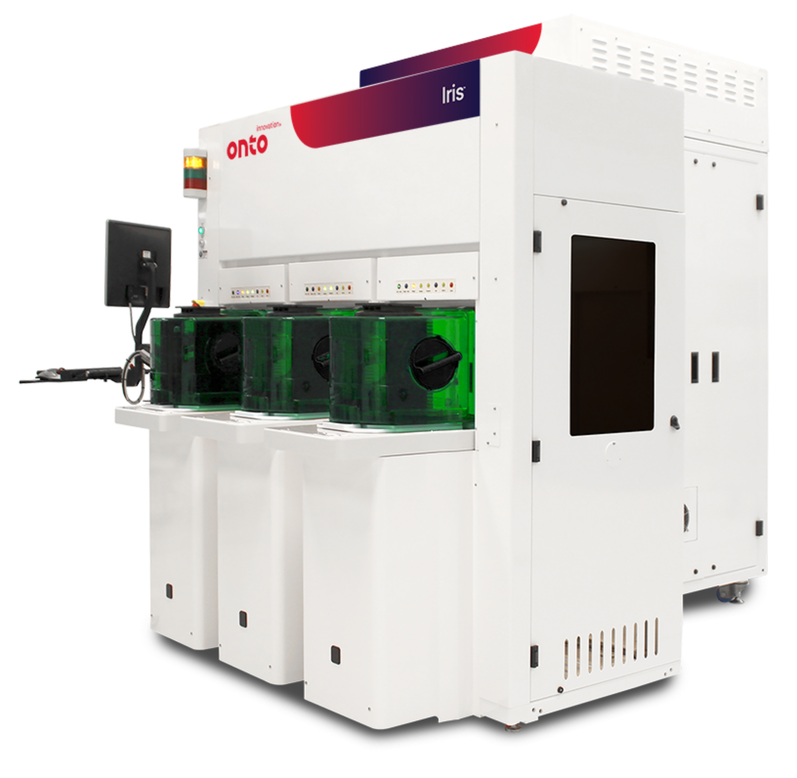
The Iris system is targeted to provide our customer the best cost-of-ownership with a dedicated application-specific optical configuration for HVM applications in semiconductor manufacturing.
The Iris C1 system combines a proprietary spectroscopic ellipsometry solution from the Atlas® family with Onto Innovation’s industry leading Ai Diffract™ OCD analysis software, enabling high precision control of every critical semiconductor process step. The system incorporates a dual-arm robot, high-precision stage and high-speed focus system. The system also features advanced pattern recognition, improved thickness reproducibility and throughput. The software interface and advanced automation are compliant with standards adopted by SEMI and other organizations. The Iris system and Ai Diffract solution provides insight of complex structure profiles across etch, clean, deposition, CMP and thin films.
Applications
- Common film measurement
- Photoresist and polymers
- Dielectric films (oxide, nitride, high-K and low-K films)
- Silicon and compound semiconductors (Si, Poly, SiGe, GaN, AlGaN, SiC, etc.)
- Silicide and metal compound
- OCD measurement
- Wafer bow, warp, and film stress
The Iris T1 is a spectroscopic ellipsometer that provides accurate, repeatable in-line thickness and optical constant measurements of single and multi-layer dielectric films for fab-wide applications. Built on the same field-proven Atlas platform, the Iris T1 system leverages the most recent advances in optics and algorithms, making it best-in-class for performance and cost-of-ownership. The SEMI/CE compliant software interface enables recipe sharing between the Iris series.
Based on a common HBLS optical design derived from our seventh generation Atlas platform and best-in-class deep ultraviolet (DUV) optics, the Iris R1 system offers maximum sensitivity and accuracy to CMP process excursions and enables device makers to establish APC control solutions with high-accuracy feedback. With SpectraProbe™ and NanoDiffract® analysis solutions enabling direct measurements within device and active areas, users are now able to monitor minor process excursions and optimize their processes for higher yields.
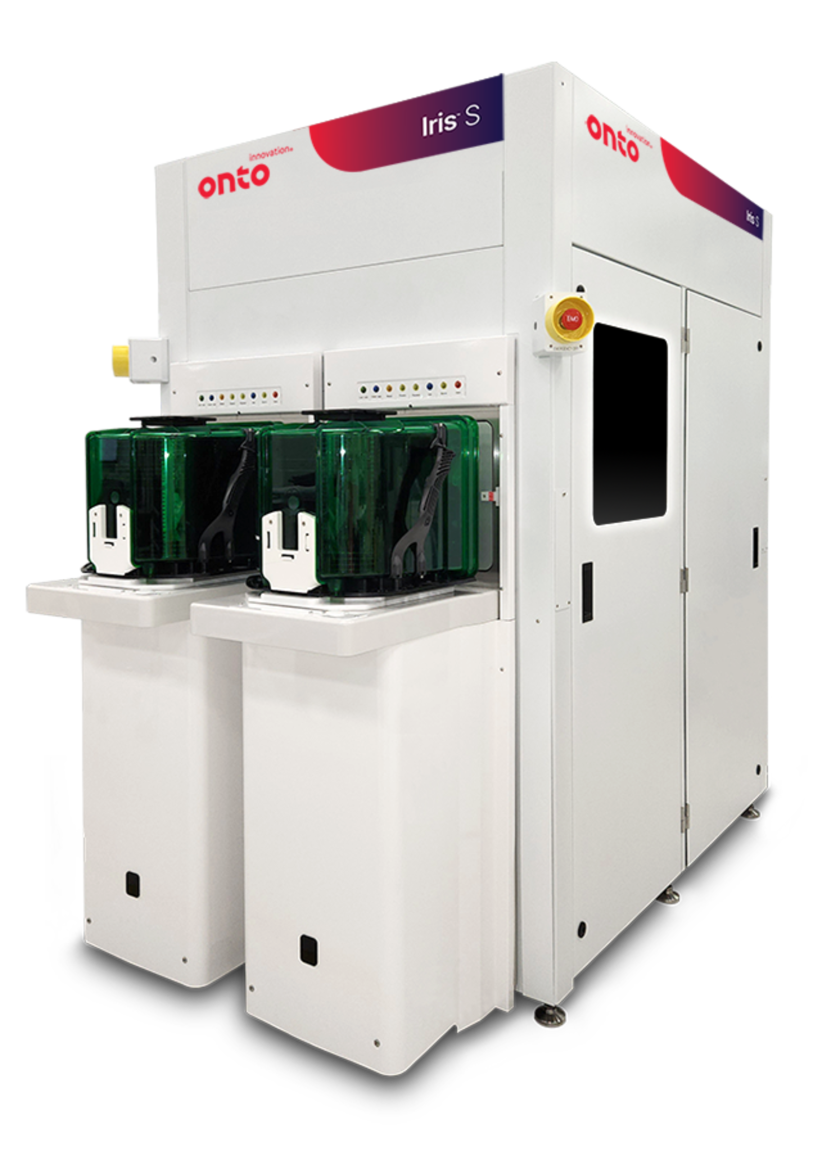
Iris S System
For SiC, GaN, glass and silicon manufacturing
The Iris S system offers a single platform solution for thin film, OCD, and wafer bow and film stress measurements on 150, 200 & 300mm wafers. It can handle a broad variety of substrates, including but not limited to SiC, GaN, glass and silicon. The system incorporates a dual-arm robot, high-precision stage, advanced pattern recognition, and a high-speed focus system for high positioning accuracy at high throughput. A state-of-the-art dual channel optical architecture offers oblique incidence Mueller Matrix spectroscopic ellipsometry (MMSE) and normal incidence spectroscopic reflectometry (SR) in a broad wavelength range from UV to IR wavelengths.
Based on the latest Windows 10 OS and a 64-bit architecture, the Ai Diffract™ software interface and advanced automation are compliant with standards adopted by SEMI and other organizations. Ai Diffract software also includes Onto’s unique model guided machine learning that enables fast, flexible and robust film and OCD recipe setup on the Iris S system.
Applications
Specifications
- Single and multi-layer common film measurement
- Photoresist and polymers
- Dielectric films (oxide, nitride, high-K and low-K films)
- Silicon and compound semiconductors (Si, Poly, SiGe, GaN, AlGaN, SiC etc.)
- Silicide and metal compound
- OCD measurement
- Mature logic
- Power
- CIS
- RF
- Other devices
- Wafer bow, warp and film stress
- Single platform for wide range of film and OCD applications
- Substrate support: 150mm – 300mm wafers with bridge capability for 150/200mm and 200/300mm
- Material handling includes Si, SiC, AlTiC, metals and glass
- Supports SMIF, open cassette and Foup loadport
- Spot size 40x40µm
- Model Guided Machine Learning enables easy system-to-system matching and seamless recipe transferability
- ISO Class 1 cleanliness
- Compliance with SE/SEMI requirements