

Understanding Optical Inspection For CIS
The demand for smartphone cameras, video conferencing, surveillance and autonomous driving has fueled explosive growth of CMOS image sensor (CIS) manufacturing in the last decade. While CIS becomes an increasingly important element in the production of today’s consumer electronics, there are unique challenges in production that must be addressed. As pixel sizes shrink, we see an inverse relationship with the number of pixels in the array increasing, which presents challenges for process control of the sensor, especially as it relates to the color filter array (CFA) and on-chip lens (OCL). With the push to 1µm and below pixel sizes, the ability to find sub-micron defects and macro-level variations within the pixel array is even more important to ensure uniform and unobstructed responses throughout the active pixel sensor array (APS).
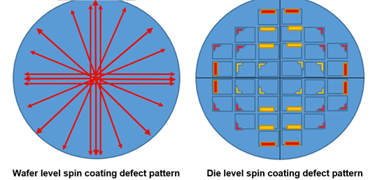
CIS is unique from other semiconductor devices because it converts light energy into electrical signals. It is manufactured on silicon wafers similar to semiconductors and follows typical back-end packaging processes such as grinding, sawing, and electrical testing. A typical CIS device has an ASP region in the center of the die with electrical I/Os (bondpads) on the periphery. Deionized water is often used to clean up mobile contamination left behind during the wafer thinning or die singulation process which has an inherent risk of staining or leaving a residue on the APS that affects the quantization of light and is considered a killer or yield limiting defect.