Series Overview
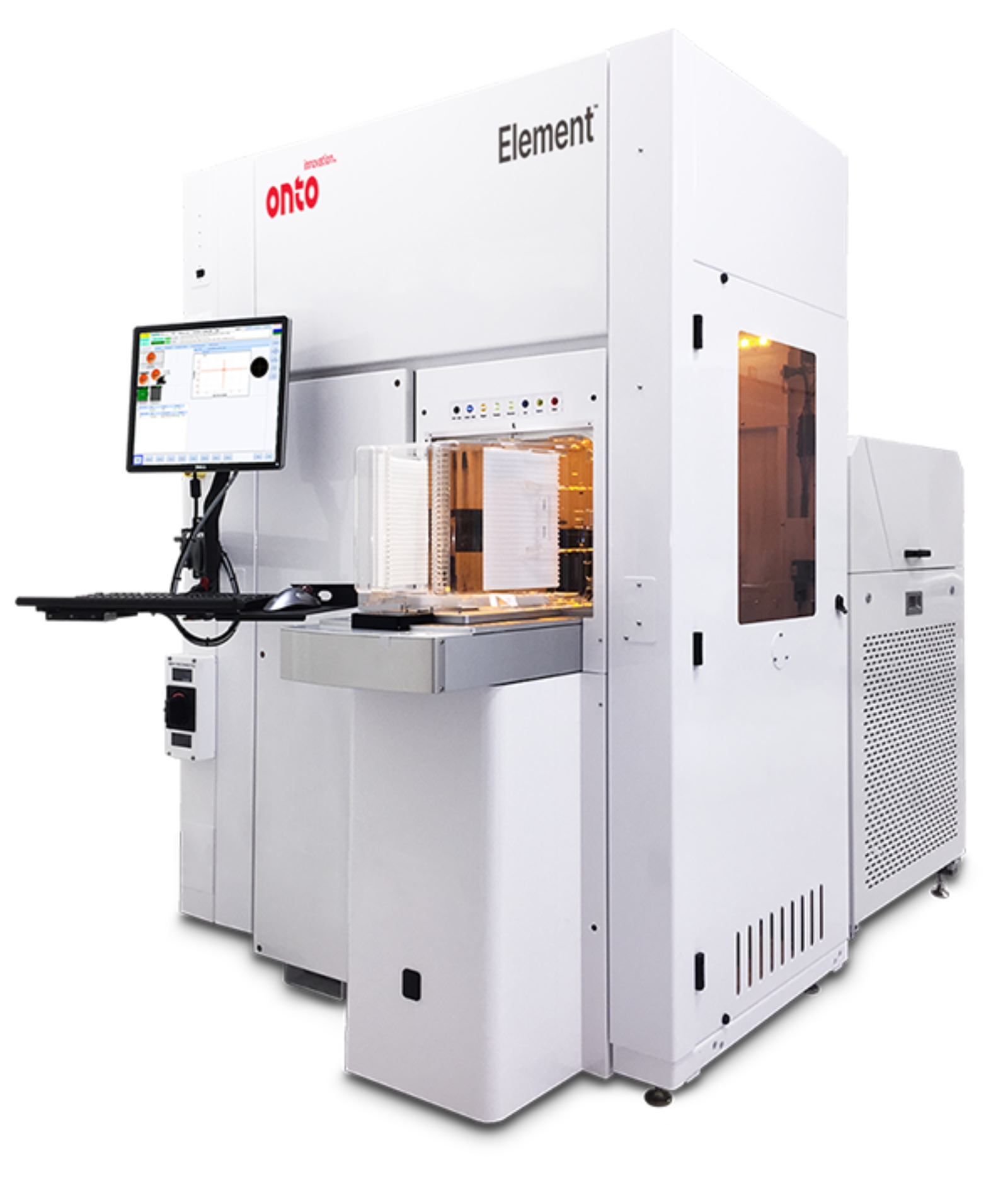
Element System
The Element system is the tool of record for wafer suppliers for high speed impurity mapping and epi thickness measurement. It is the only tool on the market with the unique combination of transmission and reflection based technology. This system is the industry standard for dielectric monitoring.
We collaborated with wafer suppliers to further improve critical wafer characteristics like epi layer thickness, epilayer resistivity and bulk resistivity using Onto Innovation’s reflection based technique.
The Element system's transmission is a classic, direct method providing best sensitivity for monitoring dielectrics like BPSG, FSG, H in SiN, etc. Machine learning is used to eliminate use of monitor wafers for dielectric measurement. Reflection only based systems do not have sensitivity to most of these dielectrics.

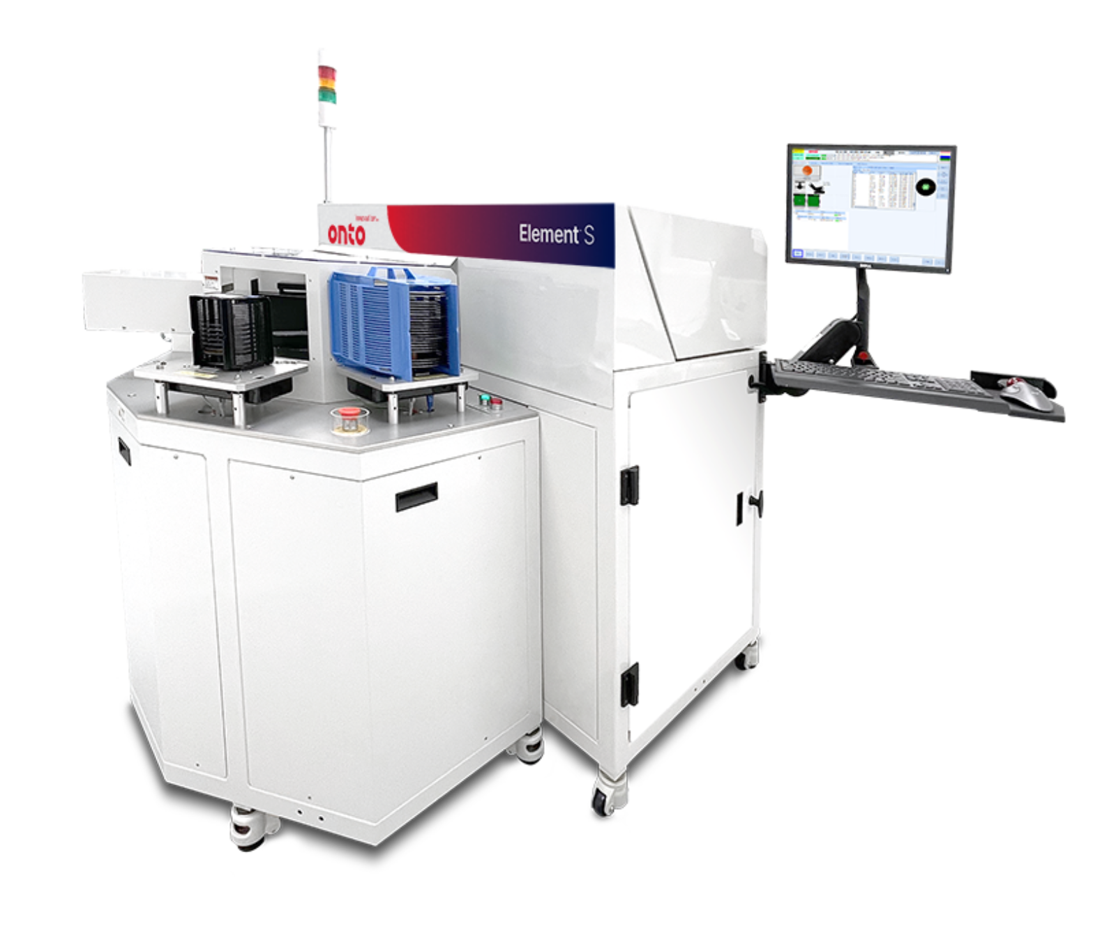
Element S System

The Element S system is designed for the specialty market, specifically the smaller 100mm to 200mm wafer sizes used in the rapidly growing SiC power device market. Building on the success of the Element Fourier transform infrared (FTIR) system, the Element S system can accurately measure thickness and free carrier concentrations in epitaxial layers up to five layers, thereby enabling the characterization of thick epitaxial films necessary for next-generation SiC power devices which require thick epi layers for higher standoff voltage. With a small spot size, the Element S system can conduct measurements up to the very edge of the wafer to maximize die yield and enable even more productivity as power device customers transition to 200mm wafers.
Applications
- Epi layer thickness
- Transition zone thickness
- Epi and substrate resistivity
- Power device
- Bulk resistivity
- Edge exclusion
- Interstitial oxygen and substitutional carbon
- BPSG – boron and phosphorus content of BPSG layers
- FSG – Fluorine content of FSG
- SiN – Measures hydrogen in silicon nitride films
- HSQ – Hydroxyl and hydrogen content in oxides SOG, FOX
- SiON – Oxygen, nitrogen and hydrogen in SiON
- SiCN – Carbon in SiCN
- SiOC – Carbon in SiOC
- Oxygen dose – Measurement of oxygen implant dose at SIMOX process
- Oxygen precipitate – Measurement of oxygen precipitates in Si substrates