

Mid-Infrared Optical Metrology for High Aspect Ratio Holes in 3D NAND Memory Manufacturing
A new metrology system uses spectroscopic ellipsometry at mid-infrared wavelengths to provide accurate critical dimension and profile measurements of high-aspect-ratio (HAR) holes in 3D NAND memory. This information is essential for developing and controlling the fabrication process. The non-destructive technique exploits unique optical properties of mid-IR radiation to extract information that has not previously been available on a robust platform suitable for in-fab use. We look at two examples: channel holes, which have aspect ratios as high as 60:1 and eventually become vertical strings of memory cells in 3d NAND memory, and the holes in the hardmask, which have aspect ratios up to 25:1 and are used to etch the channel holes.
Ellipsometric optical critical dimension (OCD) metrology in the ultraviolet to near infrared (190 nm to 1.7 mm) spectral range is a well-established process control technique. It can measure buried features inaccessible to top-down non-destructive optical, electron, or ion imaging techniques, but it has limitations when applied to the extreme 3D and high aspect ratio features of 3D NAND devices. As more devices become inherently three-dimensional and scale vertically, the ability to measure the exact dimensions of buried features and re-entrant geometries will become increasingly important.
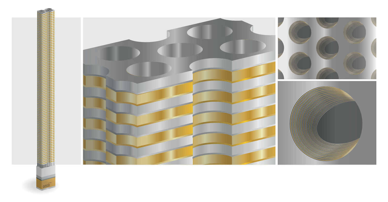
The transistor channel strings in the most advanced 3D NAND devices begin as high-aspect ratio holes (hereafter channel holes) etched through a stack of alternating silicon dioxide and silicon nitride (or polysilicon) layers with 128 or more layer-pairs. Etching holes with 100 nm diameters and depths greater than 6 mm (aspect ratios greater than 60:1) is challenging. The etch process uses a hard mask with holes of similar diameter and depths up 2.5 microns, giving them aspect ratios of 25:1 and presenting challenges similar to the channel hole etch. Figure 1 illustrates these structures schematically. An ideal etch process would yield a perfectly cylindrical hole with a uniform circular profile along its full length across the entire surface of a 300mm wafer. Realizable etch processes show significant deviations from cylindrical profiles both within a wafer and from wafer to wafer. Developing and controlling these processes requires the ability to measure hole profiles. Having this measurement capability inline accelerates process learning during the device development stage and is also critical even after the process has been transferred to high volume manufacturing where it proliferates to more etch chambers.