

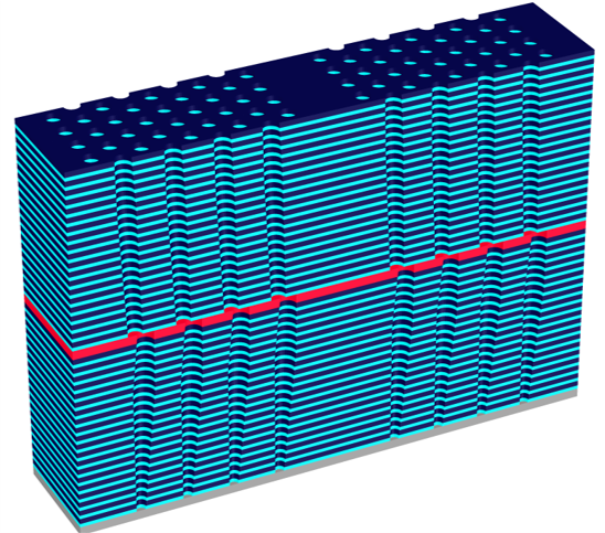
Untangling 3D NAND: Tilt, Registration, and Misalignment
The multiple demands of 3D NAND to enable yield and performance increase in difficulty at each generation. First generation devices, at 24-32 layer pairs, pushed process tools to extremes, going quickly from 10:1 to 40:1 aspect ratios for today’s 64-96 pair single tier devices. The aspect ratios increased as fast as the manufacturing challenges. To continue bit density scaling, processing improved to enable multi bit storage per layer, but still even more layer pairs are needed. With increasing layer pairs, plasma etch becomes exponentially slower.
This was quickly addressed by tier stacking—splitting the massive stack into two tiers—and it will likely increase to three or more tiers in the future. The advantage of a two-tier process is that it reduces the single etch step to a more manageable process, i.e., two 64 pair etches instead of one 128, or two 96 pair instead of one 192. 256 pair, two or three tier devices, are in development now, and 384 or more expected soon. The channel hole control improved in terms of individual profile, but at the cost of increasing device integration challenges, like adding a joint into the middle of the stack. These integration challenges are confounded by combining variation from multiple process steps. There is an increasing need to identify, measure, separate, and control each of these sources of variability.