Presentation posted on Mar 16, 2021


We will describe two major advances in ellipsometry metrology for semiconductor manufacturing: (1) development of novel optical phase-sensitive hardware incorporating the mid-infrared (IR) wavelength regime and (2) advanced machine learning (ML) solutions that are customized to overcome the perennial constraint of limited reference data.
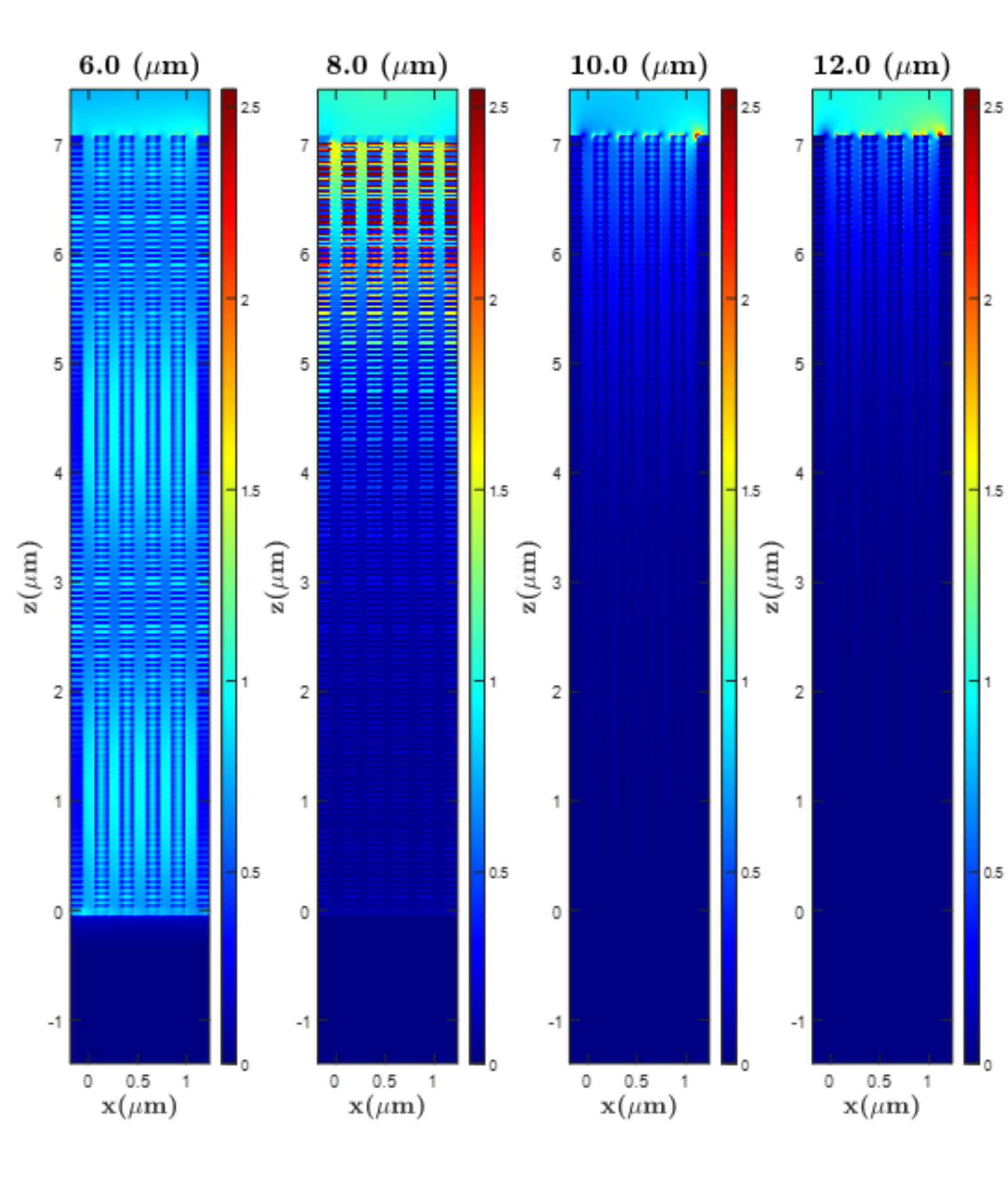
First, a novel mid-infrared critical dimension (IRCD) ellipsometry technique has been developed for the measurement of high-aspect-ratio (HAR) structures. We will show the combination of IRCD with traditional OCD technology in the UV to near-IR regime can be employed for 3D NAND channel hole etch process control with high accuracy. We take advantage of various sensitivity information at different wavelengths across this broadband spectral range to measure multiple parameters of interest (CD profile through height, tilt, and overlay) with high fidelity and nondestructively. Such a solution suite can be deployed in the development as well as high-volume manufacturing phases.
In the second half of the presentation, we will discuss how metrology-specific ML techniques can be developed with the constraint of limited reference labels, which are notoriously expensive and time-consuming because they tend to be from destructive lab techniques. We will describe two approaches to solve this problem: (1) judicious use of process skew information and (2) synergizing standard ML with physical modeling as a hybrid approach. These innovations enable pure and hybrid ML solutions to be adopted in production. Both the hardware technology and data analysis advancements are key to meet the new semiconductor metrology challenges in the most leading-edge device nodes.