Blog Post posted on May 9, 2023
No matter how you get your news, it seems like everyone is talking about AI – and it’s either going to usher in a new era of productivity or lead to the end of humankind itself. Regardless, the AI era is here, and it’s just beginning to have an impact on our lives, our jobs and our future.
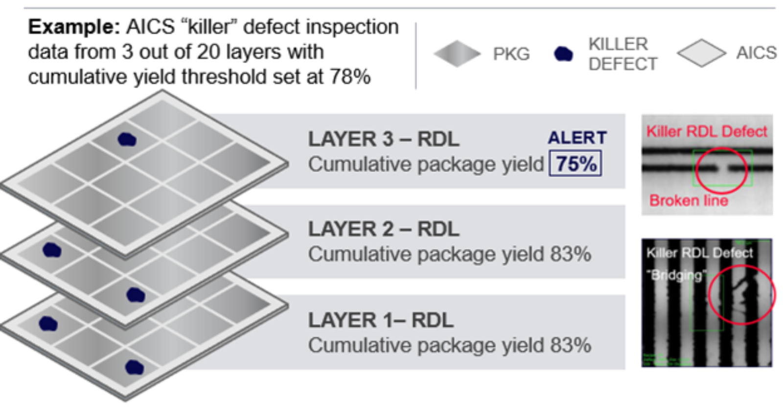
To meet the rigorous demands of AI – along with high-performance compute, 5G and electric vehicles – the semiconductor industry is seeking out new innovations to increase speed, bandwidth and functional density, lower energy usage, cost and latency. At the top of the list: heterogeneous integration. And to make heterogeneous integration a reality, back-end packaging houses use advanced integrated circuit substrates (AICS).
In a previous blog, we focused on one of the major challenges of manufacturing AICS – total overlay drift. For this second installment in our three-part series on packaging solutions, we explore the issue of AICS package yield and its importance in fostering a cost-effective, production-worthy process.