Article posted on Dec 4, 2017
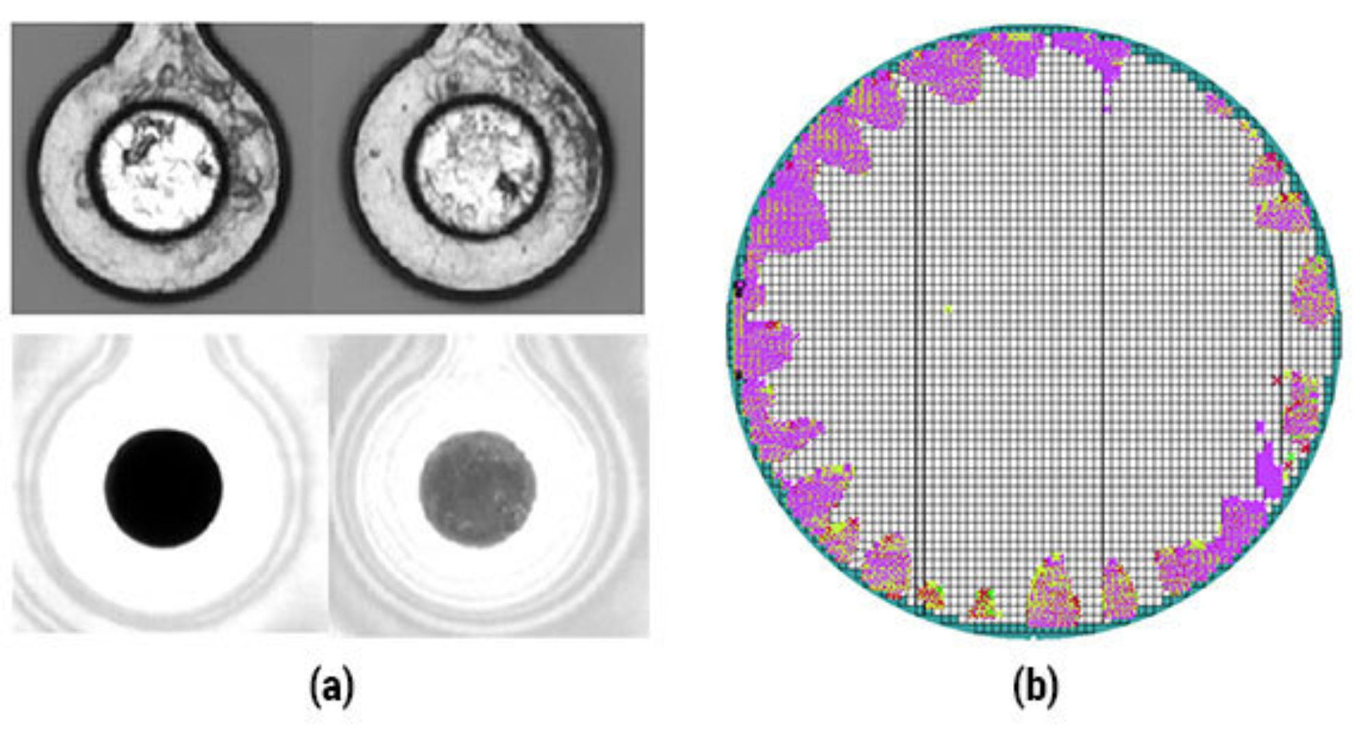
A new optical technique can reveal defects and contaminants that escape conventional inspection technologies in many advanced packaging applications. As wafer level packaging (WLP), and especially fan-out wafer and panel level packaging (FOWLP/FOPLP), gains broader acceptance, certain classes of defects that are characteristic of these processes present significant challenges to standard optical inspection tools. A new optical technology demonstrates increased sensitivity to transparent defects, such as residual dielectric films and photoresist, which are only marginally visible with conventional tools. At the same time, it is less sensitive to nuisance defects, such as those caused by the varying contrast and texture of grains in metal films, that should correctly be ignored.
The results presented here were all acquired using a Firefly™ inspection system that incorporates the new Clearfind (CF) illumination technology. The new method takes advantage of the fact that many organic polymers exhibit distinctive optical properties that are not present in metals, silicon or other common inorganic materials used in semiconductor manufacturing. These properties tend to be unique to organic molecules displaying a high degree of conjugation, such as polycyclic aromatic hydrocarbons, and in linear or branched chain organic polymers with multiple regularly interspersed pi-bonds. This phenomenon results in the generation of a readily detectable, high color-contrast signal when the feature is appropriately illuminated against a metallic or other inorganic surface. The emission tends to be anisotropic and therefore less sensitive to surface topography that could potentially direct most ordinary bright field or dark field reflected light away from the detector. This results in increased sensitivity to organic residues and reduced sensitivity to interference from surrounding features. The method has the additional advantage of being relatively insensitive to signal variations caused by metal grains.