Company News posted on Mar 19, 2019


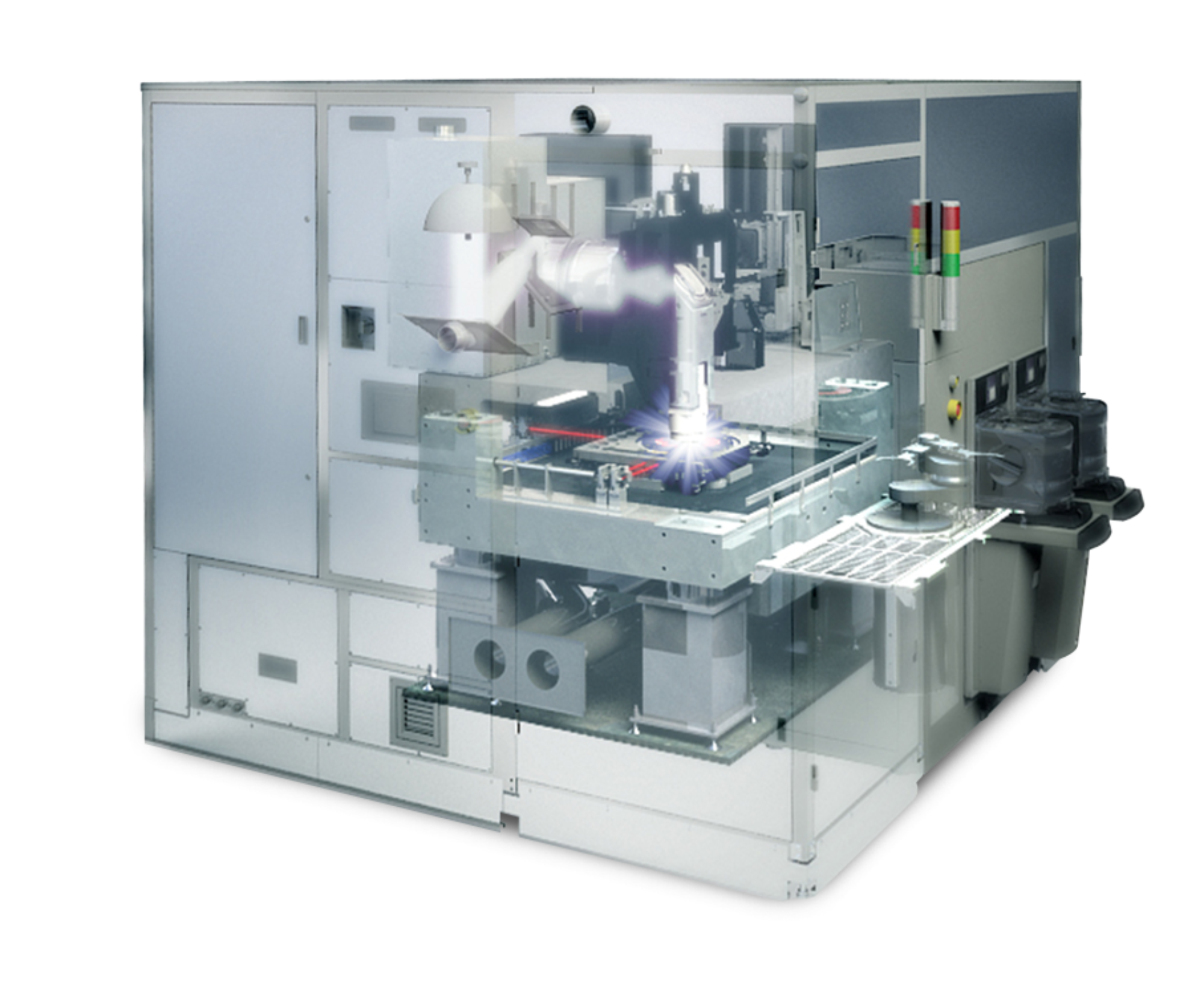
The next-generation JetStep systems feature submicron capabilities, higher throughput and lower cost-of-ownership
Wilmington, Mass. (March 19, 2019)—Rudolph Technologies, Inc. (NYSE: RTEC) today announced the immediate availability of its new JetStep® lithography systems for advanced packaging processes on wafer and panel formats. The JetStep systems incorporate an option for a new, proprietary submicron lens design, as well as up to 25% increased productivity over the previous JetStep systems. The JetStep wafer stepper will also feature a 20% smaller footprint to reduce associated cleanroom facility costs. The new systems will be highlighted at the SEMICON® China trade show March 20-22 in the Rudolph Technologies booth 4559 in hall N4.
Advanced packaging technologies, such as system-in-package (SiP) and fan-out packages (FOWLP and FOPLP) are being driven by demand from mobile, automotive and high-power computing applications. The new JetStep systems now feature a submicron lens option that accommodates critical customer roadmap requirements such as ultra-fine SiP interconnects and large-scale 50mm package sizes with significant intrafield variation. This field-proven lens with recipe controlled variable NA (numerical aperture) will allow customers to balance resolution and field size for a broader range of applications. In addition, these advanced packages now require lithography systems specifically designed to create redistribution layers (RDLs), silicon interposers, through silicon vias (TSVs), copper pillars and micro-bumps on non-flat, reconstituted wafers. Achieving this with cost in mind, the new JetStep systems include a higher power lamp and unique illumination optics that increase wafer plane light intensity by 250% over the previous JetStep systems to deliver higher productivity and throughput.
“Our latest JetStep systems provide the greatest combination of high resolution and wide field size to address our customers’ longer-range needs for finer and denser features and more integrated systems-in-packages,” said Rich Rogoff, vice president and general manager of Rudolph’s Lithography Systems Group. “The 20% footprint reduction, manufacturing-proven warped wafer handling, on-the-fly optical focusing, inter-field magnification compensation, and new edge focus and alignment capabilities result in reduced total time per wafer, and, of course, higher throughput clearly reduces cost.”
Alex Chow, Rudolph Technologies’ vice president for strategic marketing, concluded, “Next-generation packaging processes require tighter overlay and finer pitch interconnects on reconstituted wafers and panels where die have shifted from their desired position. Displacement errors can be measured on the lithography tool, but the measurements are slow, typically taking as much time as the exposure. Moving the measurement to a separate system and feeding corrections to the stepper can double throughput. Rudolph’s exclusive StepFAST™ solution is a feed-forward adaptive shot technology that addresses process variations, die placement errors and dimensionally unstable materials. This new method uses a parallel die placement measurement process and advanced analytics to provide a means to balance throughput against yield, adding an extra dimension of flexibility for optimizing profitability.”
For more information about Rudolph’s JetStep systems and StepFAST solution, visit our team of experts at SEMICON China or www.Onto Innovationtech.com.
About Rudolph Technologies
Rudolph Technologies, Inc. is a leader in the design, development, manufacture and support of defect inspection, lithography, process control metrology, and process control software used by semiconductor and advanced packaging device manufacturers worldwide. Rudolph delivers comprehensive solutions throughout the fab with its families of proprietary products that provide critical yield-enhancing information, enabling microelectronic device manufacturers to drive down costs and time to market of their devices. Headquartered in Wilmington, Massachusetts, Rudolph supports its customers with a worldwide sales and service organization. Additional information can be found on the Company’s website at www.Onto Innovationtech.com.
Safe Harbor Statement
This press release contains forward-looking statements within the meaning of the Private Securities Litigation Reform Act of 1995 (the “Act”) which include the benefit to customers of Rudolph’s products, Rudolph’s business momentum and future growth and the market demand for semiconductors generally as well as other matters that are not purely historical data. Rudolph wishes to take advantage of the “safe harbor” provided for by the Act and cautions that actual results may differ materially from those projected as a result of various factors, including risks and uncertainties, many of which are beyond Rudolph’s control. Such factors include, but are not limited to, Rudolph’s ability to plan and manage its resources and production capability, including its supply chain and fluctuations in customer capital spending. Additional information and considerations regarding the risks faced by Rudolph are available in Rudolph’s Form 10-K report for the year ended December 31, 2018 and other filings with the Securities and Exchange Commission. As the forward-looking statements are based on Rudolph’s current expectations, the company cannot guarantee any related future results, levels of activity, performance or achievements. Rudolph does not assume any obligation to update the forward-looking information contained in this press release.
Contacts:
Investors:
Michael Sheaffer
978.253.6273
mike.sheaffer@Onto Innovationtech.com
Trade Press:
Amy Shay
952.259.1794
amy.shay@Onto Innovationtech.com