Article posted on Jun 21, 2018
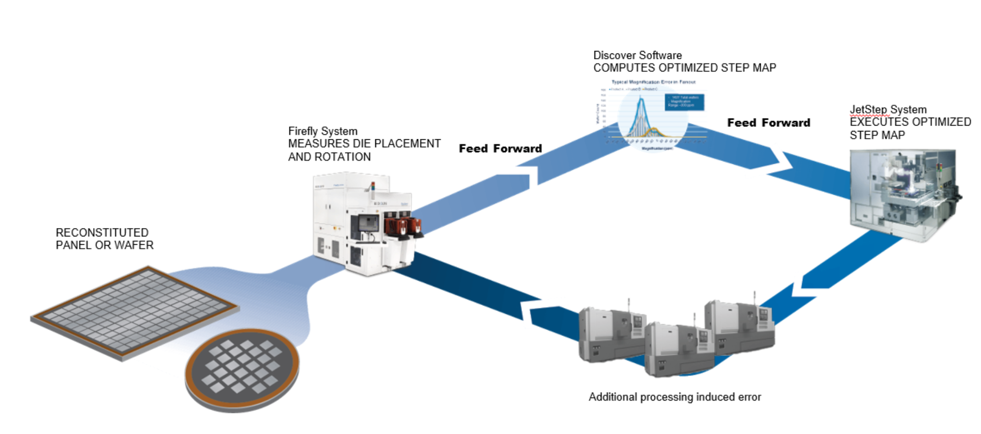
Fan out wafer and panel level packaging (FOWLP/FOPLP) processes place individual known good die on reconstituted wafer (round) or panel (rectangular) substrates, providing more space between die than the original wafer. The additional space is used to expand (fan out) the die’s I/O connections in order to create a pad array large enough to accommodate solder balls that will connect the die to the end-use substrate. The processes used to create these redistribution layers (RDL) are similar to wafer fabrication processes, using patterns defined by photolithography, with feature sizes typically ranging from a few micrometers to tens of micrometers. The placement and reconstitution molding processes introduce significant die placement errors that must be corrected in the photolithography process to ensure accurate overlay registration among the multiple vias and distribution layers that are built up to form the RDL. The errors can be measured on the lithography tool, but this significantly impacts throughput as the measurement process for each die may take as much or more time than the exposure itself.
Current best-practice methods employ an external metrology system to measure the displacement of each die. This metrology data is converted into a stepper correction file that is sent to the lithography stepper tool, eliminating the need to measure displacement on the stepper and more than doubling stepper throughput. An important enhancement to this method, optimized stepping, varies the number of die per exposure based on a predictive yield analysis of the displacement measurements, potentially multiplying throughput 20X or more. Results obtained using a test reticle that includes intentionally displaced die pads, vias, and RDL features typical of an FOWLP/FOPLP process confirm the validity of the approach.