Blog Post posted on Dec 7, 2021
The global radio frequency (RF) semiconductor market size is growing rapidly at a compound annual growth rate of 8.5%, with an expected increase from $17.4 billion in 2020 to $26.2 billion in 2025, according to Research and Markets. As many are aware, the rollout of 5G technology and the Internet of Things (IoT), which is enabled by 5G, are the main driving forces for this growth.
Growth or not, 5G devices offer their own set of challenges. These devices require up to 100 filters to isolate each RF band and avoid interferences that can drain battery life, reduce data speeds and cause dropped calls. As such, RF filters are becoming more critical for signal process applications. In the case of 5G devices, this means bulk acoustic wave (BAW) filters, which can work better at higher frequencies.
With increasingly more filters being put into devices, the size of the filters is also shrinking dramatically. In RF BAW filters operating in the 2.5GHz range, multiple channels are packed closely together, and they require frequency tolerances of <0.05% to avoid issues like crosstalk and line drops in mobile communications.
A BAW filter uses a piezoelectric film, like aluminum nitride (AlN), sandwiched between a top and a bottom electrode. This filter can be of two types: a thin film bulk acoustic resonator (FBAR) or a solidly mounted resonator (SMR). In either case the resonator needs to be acoustically isolated from the substrate. To assure a tight frequency tolerance, a frequency response must be measured. This is determined by the acoustic velocity of the AlN piezoelectric layer and the thickness of the full stack. The final frequency of each device is adjusted by adding a mass load deposited on the top electrode. This causes the downshifting of the resonance frequency. A frequency accuracy of 0.1% or better is required.
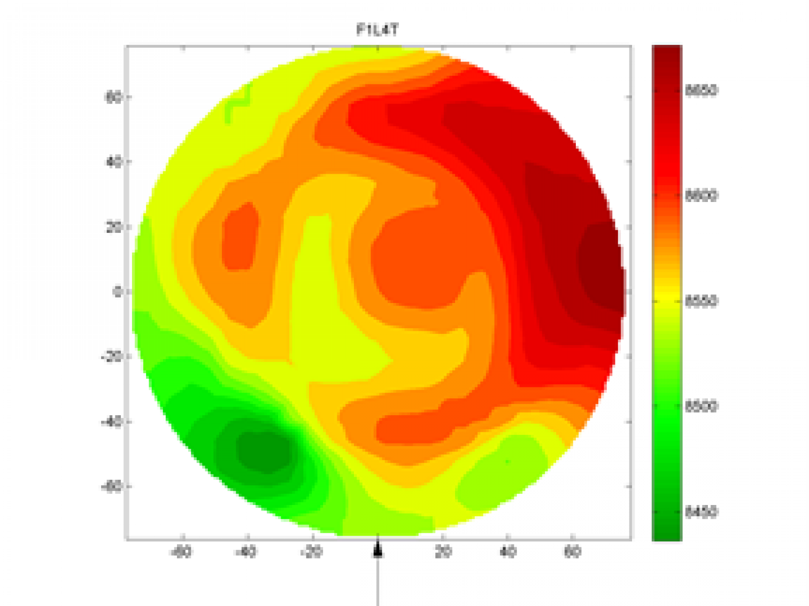
Another challenge: the uniformity of each of the layers in the stack is stringent and needs to be tightly controlled. Thin film deposition systems cannot achieve the required layer uniformity. So, tuning steps like ion milling often are introduced to achieve the desired cross-wafer uniformity.
To achieve accurate measurements, metrology techniques should meet sensitivity, accuracy, and stringent repeatability requirements. Several techniques — from sheet resistivity, X-ray fluorescence, ellipsometry and reflectometry — are available for qualifying deposition tools. However, device-level process control is required to meet yield targets. This requires measurements on the actual structures of interest to adjust the thickness via a trimming process.
Picosecond ultrasonics is a non-contact, non-destructive optoacoustic metrology that has found widespread adoption in the characterization of metal film thickness. The small spot size (8µm x 10µm) of the system enables measurements within ~0.5mm edge exclusion at production-worthy throughputs.
In RF process monitoring, picosecond ultrasonics offers significant advantages over other technologies: the ability to simultaneously measure all layers and discriminate repeating layers of the same material in a multilayer stack, the ability to measure pre-trimming to feed data to the ion trimmer for achieving desired thickness uniformity, and the ability to characterize the thickness and acoustic velocity of the piezo layer.