White Paper posted on May 28, 2018


As demand for ever more powerful personal handheld devices and advanced computing systems continues to grow, front-end manufacturers have pushed Moore’s Law to the limit and integrated more functionality into their chips while at the same time reducing their physical footprint. Modern chips are now packing more I/O channels into a smaller area than ever before. Being able to interface these devices is becoming more challenging and it is up to the advanced packaging industry to continue to develop technologies and methods to accommodate this requirement, while at the same time, reducing costs and increasing throughput.
There are inherent topographical challenges associated with the growth of 2.5D and 3D packaging where chips are placed and interconnected horizontally and vertically. The industry’s drive for cost reduction is building momentum toward large format panels and away from traditional wafers. Larger format panels are exacerbating existing issues, for example, warpage and film stresses. These variables affect the resist coating and exposure steps critical for optimal lithography. Moreover, the current liquid film application methods have encountered obstacles in meeting uniformity requirements for these large panel sizes. Non-uniform film thickness can cause processing variability and poor critical dimension control negatively impacting yield.
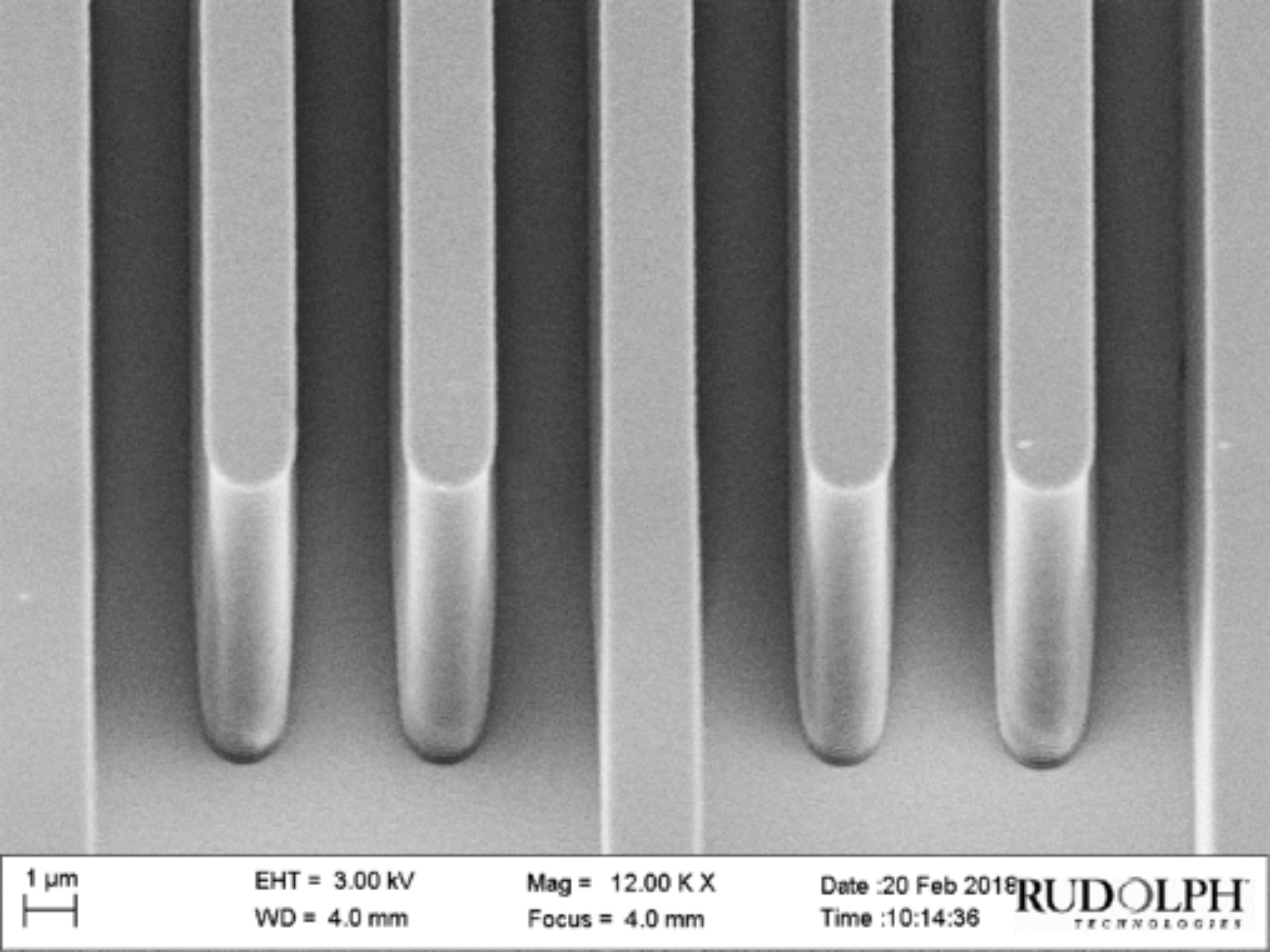
This paper demonstrates the feasibility of a revolutionary technique in the form of nozzle-less ultrasonic spray technology in conjunction with a next generation advanced packaging lithographic system for the creation of high-density, sub-2.0µm interconnects on a panel format. Performance parameters including resist thickness uniformity, sidewall angle and profile, will be compared and analyzed for this approach and other liquid film application methods. Results from the examination of the efficacy, cost reduction potential of this novel method for high-volume manufacturing will be presented.