

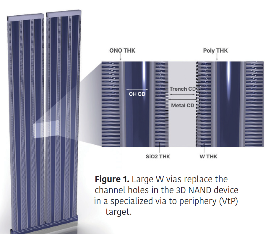
Measuring the Critical W-recess in 3D NAND
Last summer, the semiconductor industry reached a significant milestone: one of the world’s top-tier fabs had begun production of the first 3D NAND chip with more than 200 layers. The announcement was significant but not a shock. Several other fabs had been progressing toward breaking the 200-layer barrier, so reaching the milestone was not a matter of if but when.
As significant as this advance is, the high-volume manufacturing challenges of producing high-aspect ratio (HAR) 3D NAND chips are considerable. One challenge is the ability to measure the tungsten (W) recess to the bottom of a 3D NAND device following the replacement gate process. Presently, there is no in-line process control solution that can accomplish this. The reason for this is known: beyond just a few layers in the stack, the W recess becomes opaque in the ultraviolet/visible/ near-infrared region, the realm of many OCD systems, after just a few layers in the HAR stack. Additionally, increased wordline slit pitch scaling further reduces the already minimal optical signal from the top of the 3D NAND structure to the bottom.