

Large-field, Fine-resolution Lithography Enables Next-generation Panel-level Packaging
Rapidly growing demand for new types of functionality across an expanding range of applications, including 5G communication, smartphones, data centers, servers, high- performance computing (HPC), artificial intelligence (AI) and the Internet of Things (IoT), is driving a fundamental shift in the way electronic devices are designed and manufactured. Gone are the days when advances were defined by an increasing number of shrinking transistors with ever-faster switching times and lower power consumption, all fabricated as a single, monolithic integrated circuit (IC). Many of today’s most advanced systems integrate multiple die, each optimized for a specific capability and fabricated with a process designed specifically for that type of circuit. These disparate chips are then connected using advanced packaging (AP) technologies, a process known as heterogeneous integration (HI).
One example of HI uses advanced IC substrates (AICS) in a process known as ultra-high density (UHD) panel fan-out. This fan-out panel level process (FOPLP) is a redistribution lines (RDL)-first approach, where many layers of patterned conductive and insulating material are processed on both sides of a large panel to route electrical signals between the integrated chips, which are added last. Once the RDL layers are complete, solder bumps are added to form connection points that will mate with matching connection pads on the component ICs. Package substrate sizes are expected to reach 150mm x 150mm in the next few years. Panels, which may be 500mm x 500mm or larger, can accommodate many more packages per panel than the substrates used in wafer-level processes, which are restricted to round, wafer-like substrates of 300mm or less in diameter.
The lithography challenge for large heterogeneous integration is the limited size of the exposure field (typically 60mm x 60mm or less) for most currently available lithography systems. Smaller-field systems can be used to pattern large substrates by stitching together multiple exposures, but this affects both productivity and yield because of the need for multiple exposures of multiple reticles and the risk of errors at the stitching boundaries. A large exposure field would eliminate these impediments. However, there are also challenges associated with a large exposure field. These include panel warpage and distortion, which can impact critical dimensions, uniformity and overlay.
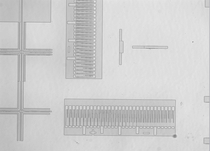
We describe here the use of our large-field lithography system (JetStep® X500) to expose 250mm x 250mm substrates in a single shot on 515mm x 510mm panels. Our evaluation included: 1) critical dimension (CD) control for 3m, 5µm and 6µm lines/spaces, and 15μm and 20μm vias; 2) CD uniformity across the exposure field; and 3) overlay accuracy. We used copper clad laminate (CCL) and Anjinomoto build-up film (ABF) panels for resolution, and glass panels with liquid resist for overlay and uniformity. The large field eliminates stitching, allows the exposure of more large package substrates in a single shot and requires fewer shots to complete a panel. We compares the exposure layout for a large field (250mm x 250mm) and a smaller field (59mm x 59mm) on a 510mm x 515mm panel. With the large exposure field, the panel can be completely exposed with just four shots, while the smaller field requires 64 shots.