White Paper posted on Jul 22, 2021


The growing demand for heterogeneous integration is driven by the 5G market that includes smartphones, data centers, servers, HPC, AI and IoT applications. Next-generation packaging technologies require tighter overlay to accommodate a larger package size with finer pitch chip interconnects on large format flexible panels.
Heterogeneous integration enables next-generation device performance gains by combining multiple silicon nodes and designs inside one package. The package size is expected to grow significantly, increasing to 75 x 75 mm and 150 x 150 mm, within the next few years. For these requirements, an extremely large exposure field with fine resolution lithography will enable packages well over 250 x 250 mm without the need for image stitching while exceeding aggressive overlay and critical uniformity requirements for these packages.
The lithography challenge to fulfill the need of heterogeneous integration is the limitation of exposure field size of the currently available solutions in the market. Multiple shots with stitching is used and this affects not only productivity performance but potential yield loss at the stitching boundary. Addressing the critical lithography challenges described above becomes an important task in heterogeneous integration, and an extremely large exposure field with fine resolution lithography is one of the best solutions for this task.
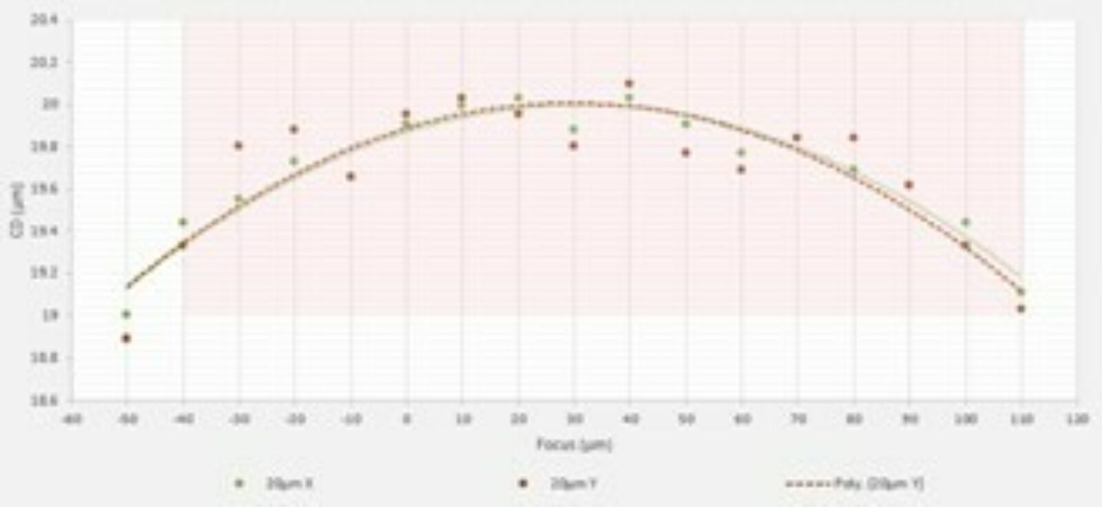
In this paper, a 515 mm x 510 mm panel is selected as the test vehicle, and we will demonstrate an extremely large exposure field with fine resolution technology on this panel. This demonstration provides the results and details about how this new technology will address the challenges of large package size processes.