

Advantages of Picosecond Ultrasonic Technology for Advanced RF Metrology
Picosecond Ultrasonics (PULSE Technology) has been widely adopted as the tool-of-record for metal film thickness metrology in semiconductor fabs around the world. It provides unique advantages, such as being a rapid, non-contact, non-destructive technology, and has capabilities for simultaneous multiple layer measurement. In this paper, we describe the unique advantages of Picosecond Ultrasonics for advanced radio frequency (RF) applications. RF filter process control requires stringent metrology due to tight process tolerances. The first principles-based PULSE technology does not require external calibration standards and provides robust measurement capability for multi-layer thickness measurements. For advanced RF applications, the capability of PULSE technology to measure both velocity and thickness simultaneously for transparent and semi-transparent films offers a lot of potential for not only monitoring processes but offers insight into the device performance. The PULSE technique can also simultaneously measure full stack for multilayer metal stack measurements with excellent repeatability and long-term stability which makes process control more efficient and reliable. Fast throughput makes it possible for a high sampling rate for RF applications which is the key for device level process control and yield improvement.
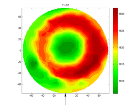
The global RF semiconductor market size is growing rapidly at a CAGR of 8.5% in the next five years from 17.4 billion in 2020 to 26.2 billion USD in 2025. The rollout of 5G technology and its enabled Internet of Things (IoT) are the main driving force for this growth. Each 5G device requires up to 100 filters to make sure each band is isolated to avoid interference that will drain battery life, reduce data speeds, and cause dropped calls. RF filters are becoming more and more critical for all signal process applications. 5G devices require Bulk Acoustic Wave (BAW) filters which can work better at higher frequencies. With more and more filters to fit into a device, the size of filters is also shrinking dramatically in three dimensions. These advances in filter technology place stringent demands on manufacturing which in turn requires accurate and precise metrology techniques. Both thickness and acoustic properties of the piezoelectric layer determine the frequency response of filters. Thickness accuracy and uniformity requirements for the films are beyond what process tools can offer at deposition and there are several options available to achieve such tight controls post-deposition. Metrology techniques employed for characterizing these properties must meet the sensitivity, accuracy, and stringent repeatability requirements. The thickness of the full stack and especially the thickness and sound velocity of the piezoelectric layer are key to realizing the extremely tight process control of frequency accuracy (3σ) of 0.1% or better. A high sampling rate on a hundred-micron level device is needed to make sure all devices across the wafer can meet the requirements which require fast throughput with a small measurement probe.