Blog Post posted on Nov 7, 2023
Wind power. Rail. Solar energy. And, perhaps most significantly, electric and hybrid vehicles. Together, these four forces are among the major demand drivers for power devices.
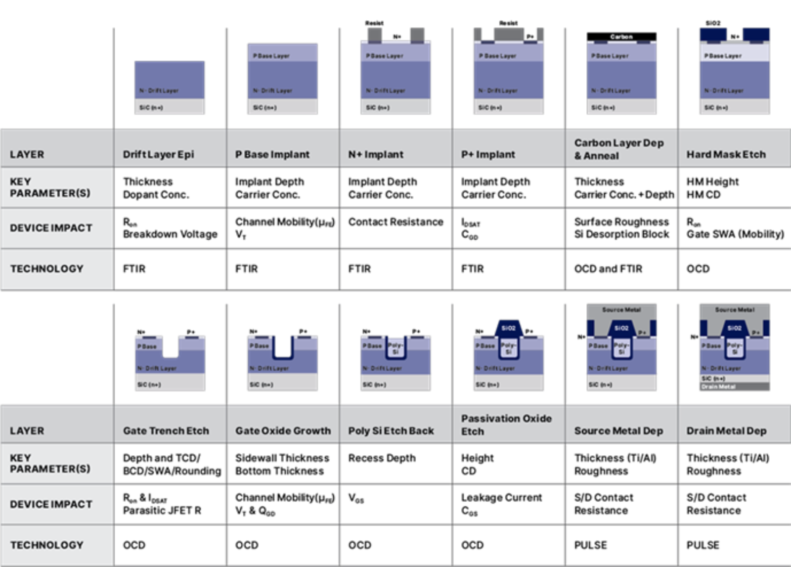
While silicon (Si) still plays a role in power devices, wide-bandgap compound semiconductors like silicon carbide (SiC) and gallium nitride (GaN) are particularly well-suited for power devices thanks to their higher electron mobility, higher critical electric field and higher thermal conductivity. However, as new structures and larger wafer sizes become the norm for power devices, they bring with them distinct manufacturing challenges.
Today, the industry is transitioning from 150mm to 200mm wafers for SiC- and GaN-based devices and 200mm to 300mm wafers for Si-based devices. The reason: larger wafer sizes may help reduce the cost of fabrication. As the wafer size transition occurs, it is important to have a metrology tool that can measure a larger number of data points across the wafer without impacting the overall fab throughput. A loss of throughput adds to cost-of-ownership and may erase savings earned from transitioning to larger wafers.