Blog Post posted on Mar 7, 2023
For years, many in the semiconductor industry have focused on the march toward advanced nodes. As these nodes have decreased in size, the size of input/output (I/O) bumps on the chip has grown smaller. As these bumps shrink, their ability to mate directly to printed circuit boards (PCB) diminishes, which, in turn, leads to the need for an intermediary substrate. Enter the advanced IC substrate (AICS).
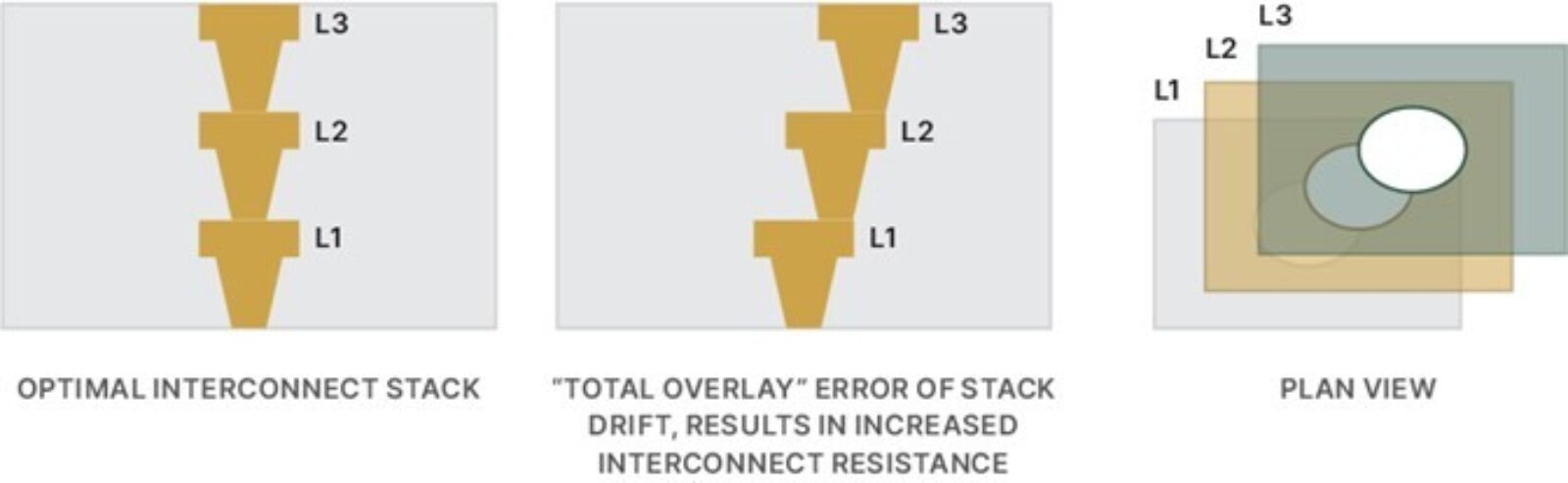
The use of AICS also enables advances in panel-level packaging and the rise of chiplet-based architectures, where the final product is an assembled composite of multiple die supporting the core central processing unit (CPU) or graphics processing unit (GPU). These additional die may be memory elements, analog devices or other functions. All these die can be co-packaged on the AICS, which allows multiple die with small I/O contacts to be assembled and redistributes them to larger contact bumps compatible with a PCB.
With panel-level packaging, manufacturers can deliver packages offering faster data transfer, greater heat dissipation, less power consumption and increased functionality. And unlike the front-end where higher resolution involves ever smaller patterns, package sizes are only increasing in size.