Blog Post posted on Jun 11, 2024
Whether the discussion is about smart manufacturing or digital transformation, one of the biggest conversations in the semiconductor industry today centers on the tremendous amount of data fabs collect and how they utilize that data.
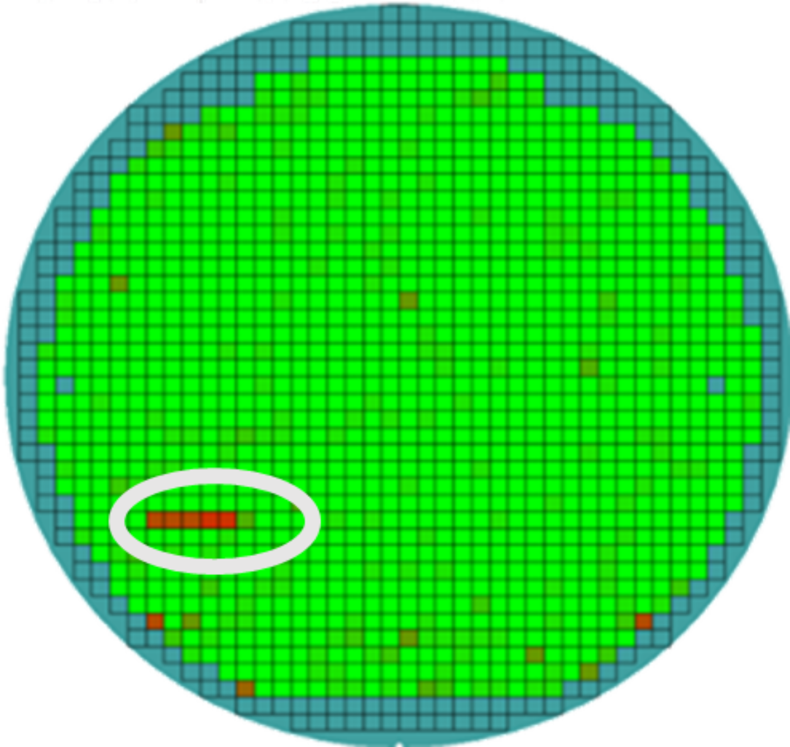
While chip makers are accumulating petabytes of data across the entire semiconductor process, a question arises: how much of that information is being fully utilized? The answer may be around 20%, according to the Semiconductor Engineering article “Too Much Fab and Test Data, Low Utilization.” Unfortunately, this poses a challenge because fab end customers are demanding highly reliable chips, in other words, chips with zero escaping defects and which offer manufacturers clear genealogy and traceability.
Many of you reading this work for companies that have started or are planning digital transformations. To do this, these companies will need to better integrate the data they collect — and that includes data from materials, products, processes, factory subsystems and equipment.
For smart manufacturing to truly live up to its potential, manufacturers will need inline automation that takes complete advantage of the analytics their monitoring systems generate, analytics which can be fed back to the process tools, manufacturing execution systems and other factory systems in real time. Working in concert, these integrated systems are essential to creating a zero defect manufacturing environment.
In the world of smart manufacturing, manufacturers will be tasked with providing timely total solutions to detect and classify defects using inspection and metrology tools, conduct root cause analysis to determine the source of said defects and, finally, employ process control and equipment monitoring using run-to-run and fault detection and classification software solutions to prevent defects from reoccurring.
In this blog, the first in our three-part series “Achieving Zero Defect Manufacturing,” we will focus on detecting and classifying defects. We will start by looking at solutions at the defect level before moving on to the die level and the wafer level.