A Bare Wafer Mystery: Inspecting for Back, Edge and Notch Defects in Advanced Nodes

It is no mystery that the semiconductor industry is always advancing, with specifications becoming increasingly stringent as defects become increasingly more difficult to discover. This is especially true in the case of the most advanced nodes, where ever-smaller flaws and deformities can result in a killer defect.
To solve this More than Moore mystery, you do not need to employ the detective skills of Sherlock Holmes. You need the metaphorical equivalent of the pipe-smoking hero’s magnifying glass to find the particles, scratches, pits and air pockets hiding in the shadows.
Take the critical dimensions of trenches and vias, for example. As they shrink, the size of a particle or scratch that can potentially result in a killer defect decreases in size as well, making sensitivity an increased priority for bare wafer inspection — on the frontside and backside, at the edge and in the notch.
With an eye on evolving requirements for advanced node bare wafers, manufacturers are seeking inspection solutions with automatic defect classification (ADC) capabilities to perform outgoing quality assurance for wafers, including polished wafers and those with silicon epitaxial layers. Armed with these ADC capabilities, customers can significantly reduce the need for time-consuming and costly manual review.
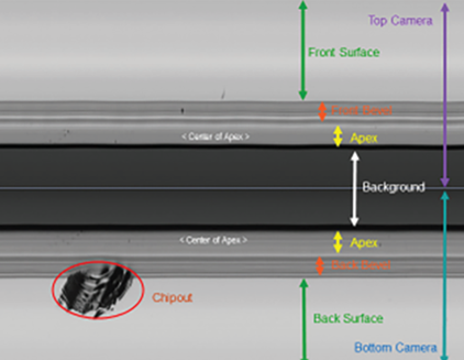
The frontside, bulk, backside, edge and notch — each of these areas needs to be inspected to ensure the quality of the silicon wafer and the successful fabrication of advanced devices on the wafer. We’ll start with frontside and bulk before moving onto backside, edge and notch inspection, the main focus of this blog.

