Picking up the Pace of Panel-level Advanced Packaging at Onto Innovation

Panel-level advanced packaging technologies have been in development for more than a decade. They began as a way to reduce costs and improve yields for fan-out wafer level applications. Smartphone applications – particularly fingerprint sensors – promised the volumes that would make the investment successful.
However, memories of the fiasco of 450mm wafer efforts lived in the minds of many. Why make the investment in an ecosystem that may not demand high enough volumes to insure return on investment? Still, there were those who believed in the promise of panel-level packaging. Development efforts persevered, and PLP has moved through R&D and into pilot production. Still, through it all, many remained skeptical about there being high enough volumes to support it.
The Era of AI, coupled with the emergence of glass substrates, is set to change all that.
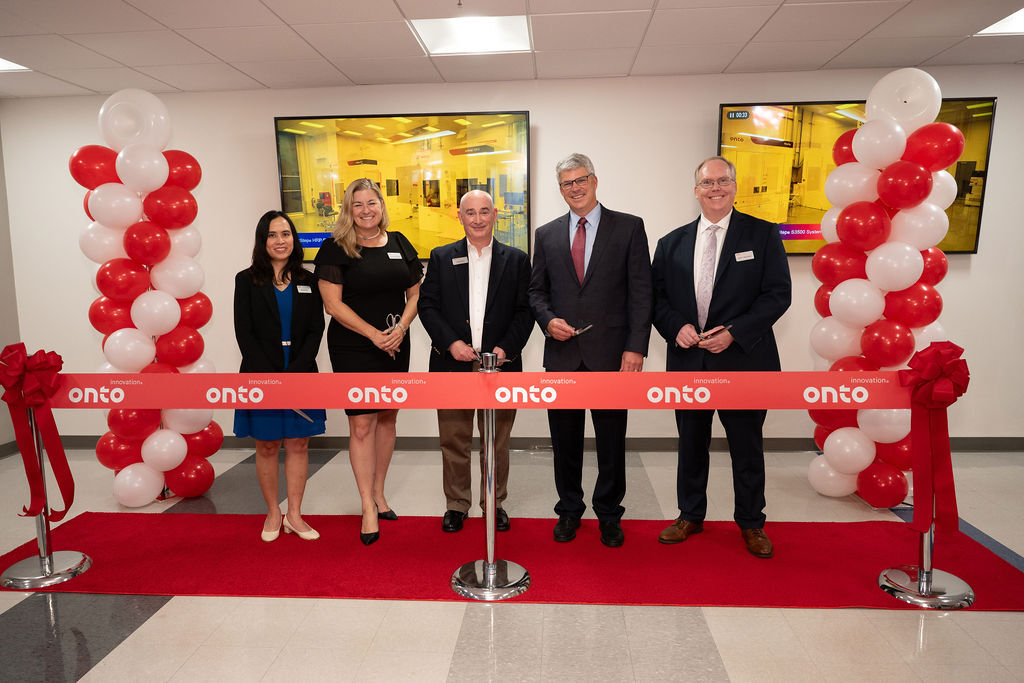
On September 30, 2024, I visited Onto Innovation’s headquarters in Wilmington, MA to attend the grand opening of its Packaging Applications Center of Excellence (PACE). The company has partnered with like-minded suppliers of the PLP ecosystem to accelerate the development of PLP technologies for both organic and glass substrates. These include 3D InCites Members: LPKF Laser & Electronics, Evatec, MKS-Atotech and Lam Research; as well as Resonac, Corning, and others.

