Metrology Solutions for Advanced Packaging
Your partner for today's metrology challenges
Your partner for today's metrology challenges
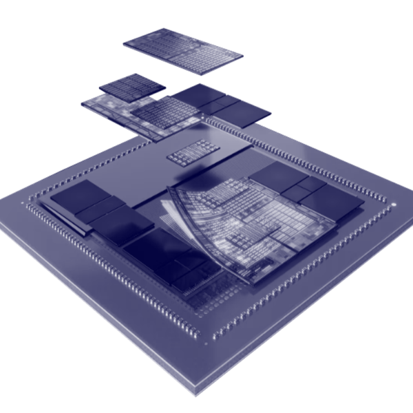
Today's advanced packaging processes that involve 2.5D or 3D integration via bumping, through silicon vias or hybrid bonding require process control metrology to help ensure each die's interconnects are reliable. Onto Innovation is a leader in process control metrology partnering with manufacturers to solve the industry's most advanced challenges for next generation devices.
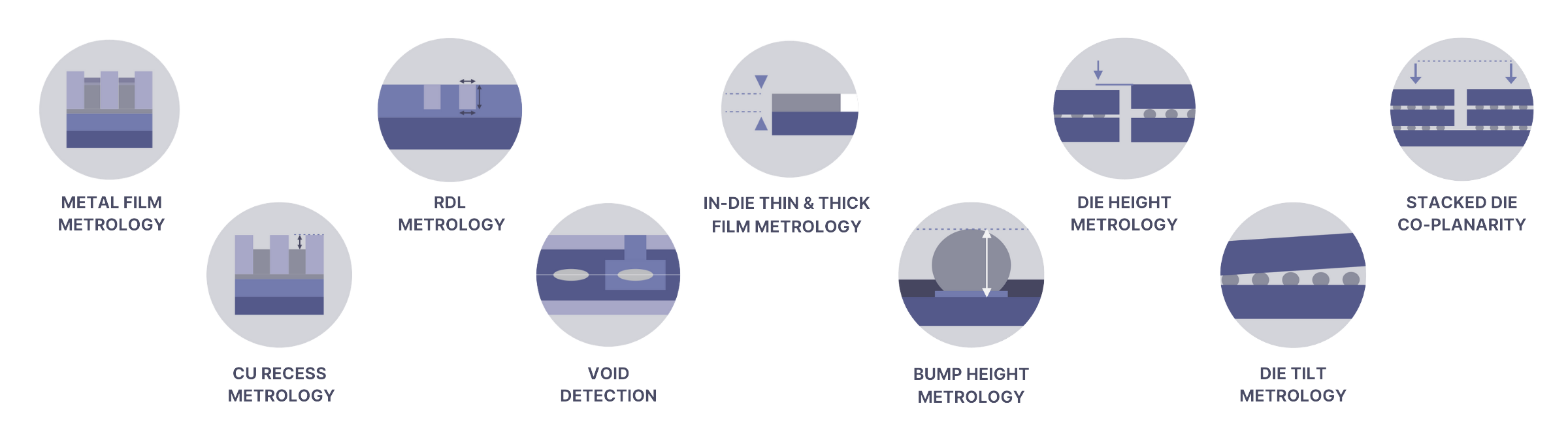
Process challenges, ranging from films metrology to void detection, present an opportunity to improve yield and reliability with the proper metrology techniques in place. Learn more about Onto's solutions below.
Whether performing metrology on the wafer or die level, Onto Innovation has you covered. Our broad portfolio serves both macro and micro levels required for steps in advanced packaging.
Non-destructive in-die multi-layer metal film thickness measurement.
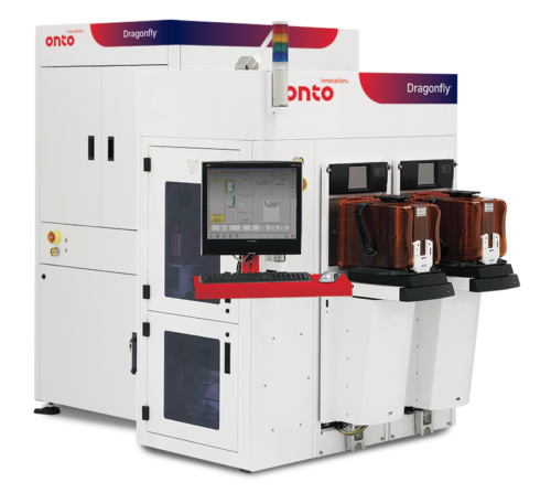
Versatile optical metrology system designed for the diverse needs of advanced packaging applications, including thin and thick films, TSV, RDL and Cu recess.
Measure co-planarity and die tilt when stacking die to help ensure proper alignment for performance reliability of the package.
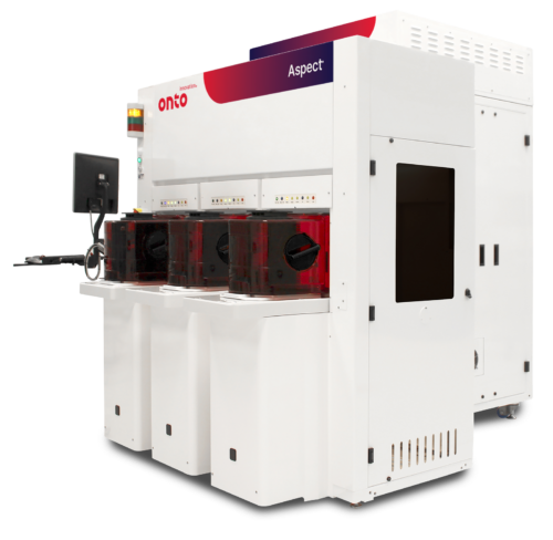
Mid IR OCD system with differentiated performance on high aspect ratio (HAR) and large pitch devices, including µTSV profile and Cu recess.