‘XL’ Fine Resolution Large Field Lithography Dramatically Cuts FOPLP Pattern Distortion

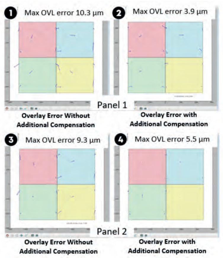
Heterogeneous integration enables multiple chips from varying Silicon processes to deliver superior performance. In large panel packages, present day limits on exposure field size forces manufacturers to ‘stitch’ together multiple reticles, which slows throughput and increases costs. Onto Innovation’s new JetStep® X500 system dramatically increases the exposure field up to 250 x 250 mm, slashing the number of exposures needed and cutting costs in FOPLP applications.
HIGH-PERFORMANCE compute, 5G, smartphones, data centers, automotive, artificial intelligence (AI) and the Internet of Things (IoT) – all rely on heterogeneous integration to achieve next-level performance gains. By combining multiple silicon nodes and designs inside one package, ranging in size from 75mm x 75mm to 150mm x 150mm, heterogeneous integration is one factor bringing us closer toward an era in which technology is beneficially embed into nearly all aspects of our lives whether it’s in the smart factories where we work, the self-driving cars that navigate the cities in which we live, the mobile devices that connect us to each other and the wearable devices that help us live healthier lives.
Regardless of the speed to which we are approaching this promising new era, this transition comes with increasing challenges, ones that are constrained by increasingly stringent requirements. The next-generation of heterogeneous integration technologies, and the fan-out, panel-level packaging that often accompanies it, will demand even tighter overlay requirements to accommodate larger package sizes with fine-pitch chip interconnects on large-format, 510mm x 515mm flexible panels.

