Blog Post posted on Jul 6, 2021


When it comes to multi-chip module (MCM) manufacturing, fan-out wafer-level and fan-out panel-level packaging have received a lot of coverage recently. Every week, it seems like there is an announcement about “Company XYZ” moving their products into the fan-out wafer-level packaging (FOWLP) or fan-out panel-level packaging (FOPLP) space. But these moves come with challenges that didn’t exist in the advanced packaging assembly space years ago. And it’s these challenges that today’s MCM manufacturers need to address.
Consider this: at the most ambitious panel manufacturing facilities, masking layers may now number a dozen or more layers. Couple that with the fact that there may be more than 60 days of cycle time at some FOWLP facilities, and it becomes clear that the issues MCM factories need to address are looking similar to the issues front-end (FE) fabs faced in the 1980s.
Back then, FE operations drove many of the requirements — from factory automation to data collection and analytics — that we take for granted in today’s semiconductor industry.
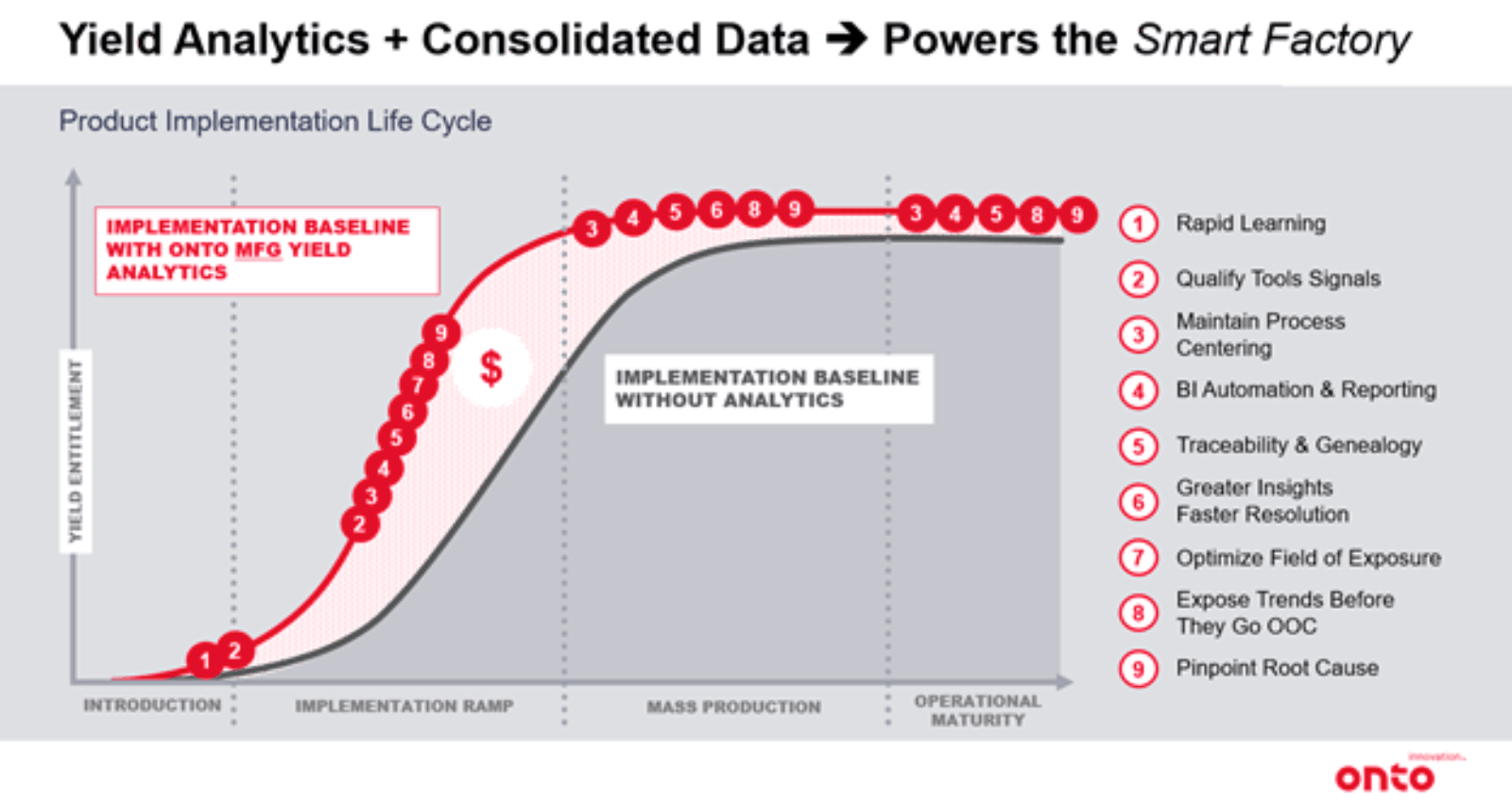
The reasons why defect and yield management systems were important to fabs in the 1980s are the same reasons defect and yield management systems are needed now at MCM factories. This holds true for die-first fan-out wafer-level manufacturing and die-last fan-out panel-level manufacturing.
When it comes to FOWLP manufacturing, the operational processes are similar to the operational processes used in semiconductor manufacturing, with lithography, film deposition and etching all playing roles. The two manufacturing environments have several common steps, film etching and polishing being the most obvious. Much like the FE, these MCM tools need dynamic controls and run-to-run management in order to properly function, day in and day out. These facilities can leverage the lessons that have been learned from decades of excursion events and ever faster yield ramps in FE fabs by including integrated metrology defect and yield systems during the initial MCM facility build out.