Blog Post posted on Jan 9, 2024
The figures alone are impressive: SiC power devices are experiencing an annual average growth rate approaching 34% through 2027, according to the Yole Group. However, the potential for this amongst other compound semiconductor-based power devices such as gallium nitride (GaN) to change the world around us is even more impressive.
Thanks to the role that SiC-based devices play in the increased electrification of automobiles and the sustainable energy movement, the effort to make this world a cleaner, greener place is no longer a wished-for science fiction fantasy. It may one day be our reality. Perhaps even soon.
Manufacturers in the automobile and clean energy sectors want power devices that are more efficient and can accommodate higher voltages, faster switching speeds and lower losses than traditional silicon-based power devices. To accomplish this, they are turning to higher efficiency silicon carbide (SiC)-based devices.
When it comes to SiC power devices, most manufacturers have adopted a trench-based architecture. This reduces on-resistance and increases carrier mobility. However, these improvements come at the expense of rising fabrication complexity.
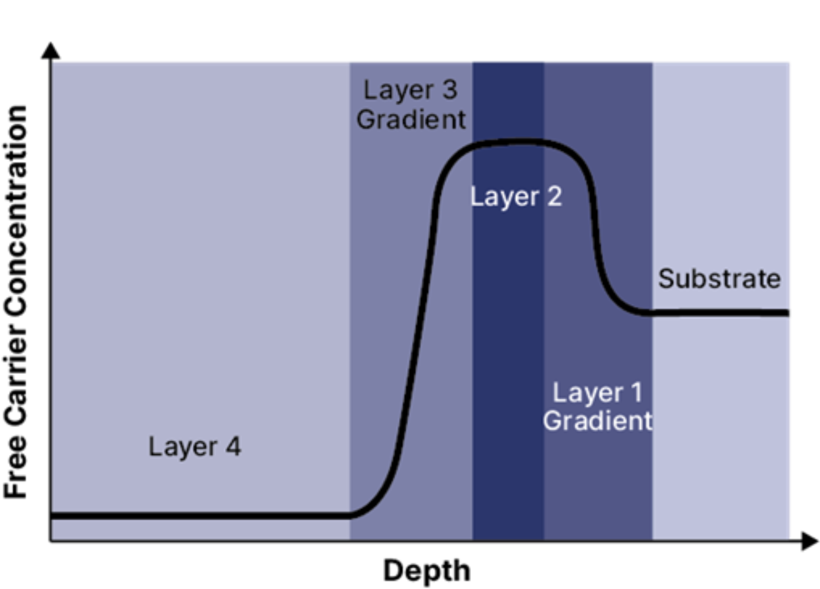
To address this issue, high-volume manufacturers of SiC power devices are, at several key steps, adopting inline process control methods, including optical metrology techniques like Fourier transform infrared (FTIR). With a system supporting FTIR optical metrology at their disposal, manufacturers can more accurately measure epi layer growth and the depth and accuracy of implanted dopants across the wafer, key challenges posed by the increased fabrication complexity of SiC power devices. In this blog, we’ll discuss how FTIR technology can help manufacturers successfully address these challenges.