

Using Deep Learning ADC for Defect Classification for Automatic Defect Inspection
Abstract
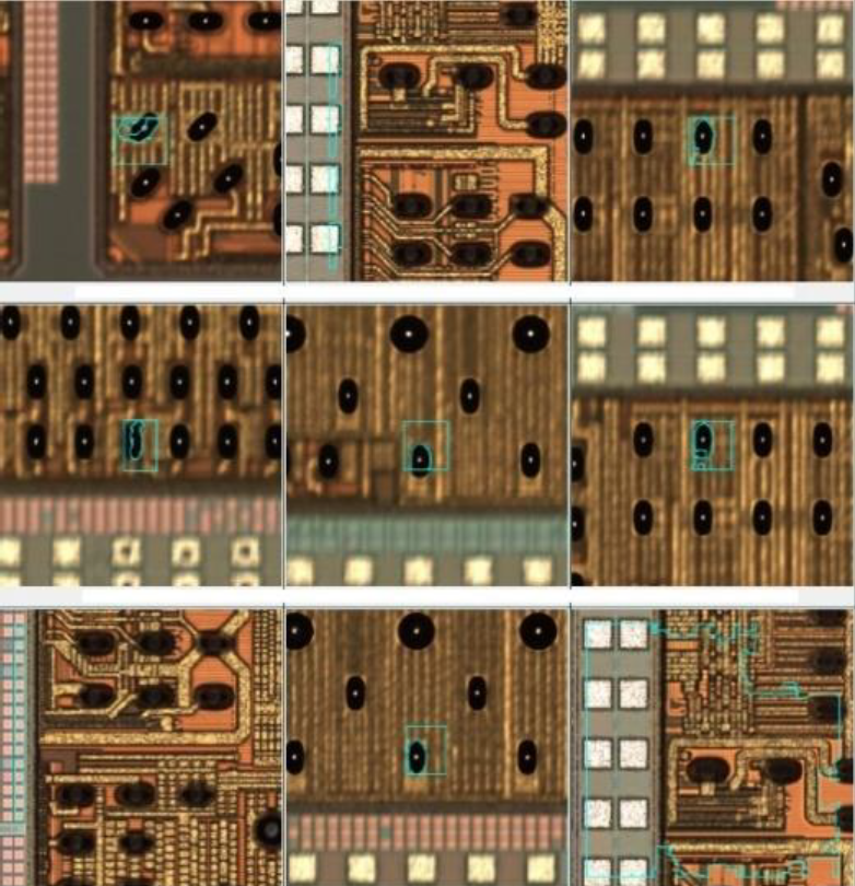
In traditional semiconductor packaging, manual defect review after automated optical inspection (AOI) is an arduous task for operators and engineers, involving review of both good and bad die. It is hard to avoid human errors when reviewing millions of defect images every day, and as a result, underkill or overkill of die can occur. Automatic defect classification (ADC) can reduce the number of defect images that need to be reviewed by operators. The ADC process can also be integrated with AOI engines to reduce nuisance defect images to reduce AOI image capturing time. This paper will focus on how to utilize Onto Innovation’s TrueADC software product to build ADC classifiers using a multi-engine (ME) solution. The software supports CNN, DNN and KNN algorithms. The use of CNN and DNN are currently mainstream in the development of deep learning (DL) for ADC classification in the semiconductor industry. We will address how to improve classification by using multiple models in the classification process with unique algorithms. As a result, the user can achieve industry requirements with very demanding specifications, like high accuracy, high purity, and high classification rate with very low escape rates.