Blog Post posted on Oct 15, 2024
The semiconductor industry is a land of peaks and valleys. It’s a place where each innovation represents the culmination of a long and often difficult climb to the summit. In the case of glass substrates, the peak of the mountain is in sight.
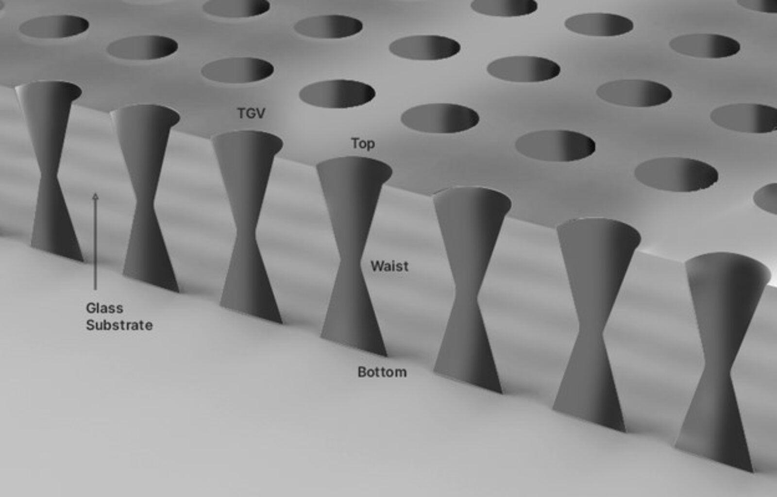
The arrival of glass substrates comes at an opportune time, as the industry eyes new process innovations to meet the incredible demand for high performance applications, like AI, and their stringent requirements, including further decreases in size and pitch for through glass vias (TGV). Up until now, organic substrates employed plated through hole (PTH) type vias , but these will be unable to meet these challenging requirements.
With the advent of glass core substrates replacing organic substrates, various processes hitherto requiring basic printed circuit board (PCB) technology take on a new dimension with significantly greater complexity. This blog discusses the formation of interconnects through the substrate, whether those interconnects are PTH for organic substrates or TGV in glass substrates.