

Outlier Control Technology and Feedforward Lithography Can Boost FOPLP Yield
FAN-OUT PANEL LEVEL PACKAGING (FOPLP) has multiple benefits in advanced packaging applications, including enhanced connectivity and reduced costs. FOPLP differs from wafer-level packaging processes in that FOPLP utilizes large, rectangular panels rather than the round silicon wafers typically associated with IC manufacture. FOPLP’s rectangular panels more efficiently fit rectangular die, which can reduce costs since manufacturers can process more packages in each run.
Despite many advantages, FOPLP also faces specific challenges, such as yield loss caused by inaccurate die placement and the resulting overlay errors. In this context, dies with unusually large placement errors, or outliers, can be especially troublesome. These outliers cause losses of both the misplaced die and surrounding dies. However, integrating outlier control with feedforward metrology can greatly improve both yield and throughput.
Fan-out processes cut individual dies from the wafer and reconstitute them on a processing substrate separated by additional space. Subsequent steps fabricate redistribution lines in multiple layers and end with the creation of contacts on the surface of the package. The area available for contacts is increased by the additional space between chips, allowing more contacts per chip.
One critical challenge for FOPLP is die-placement error. This error originates during the robotic pick-and place operation in which chips are positioned on the reconstitution substrate. The problem arises when die positions shift during subsequent processing steps. If uncorrected, these die-placement errors can result in overlay errors and reduced yield. While die-placement errors can be measured and corrected, die-by-die in the lithography tool, this greatly reduces throughput. Feedforward lithography, which measures placement errors and calculates corrections in a separate system and then feeds the corrections forward to the lithography system is much faster. Lithography throughput can be further increased by including more than one die in each exposure site and then applying site-by site corrections to the exposures.
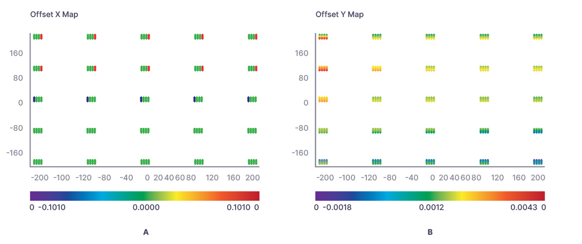
In this scheme, dies with unusually large placement errors can have an outsized impact on yields by skewing the site correction to such a degree that the site correction causes unacceptable overlay errors for all dies in the site. A solution: advanced outlier control technology (Figure 1). This technology detects outliers and excludes them from the correction calculation, thereby sacrificing the outlier to optimize overall yield and throughput.