White Paper posted on Mar 4, 2018


Advanced packaging technologies require materials that will allow for better resolution of patterns associated with the ever more challenging device architecture, along with materials that will allow for higher throughput. Device throughput can be increased with imaging materials that have higher sensitivity. Chemically-amplified photoresists offer the advantages of excellent sensitivity and resolution with good process margins, coupled with excellent stripping performance and plating bath compatibility for the film thicknesses that are required in packaging applications. However, it is the integration of the photomasking material and the availability of today’s advanced back-end exposure tools that allow for improved lithographic imaging. It is this combination that is necessary for meeting the demands of today’s higher resolution and tighter pitch requirements for back-end plating applications, which is essential in producing metallized structures for copper pillar and solder applications. Because the profile of the resist image is directly transferred during the electroplating process, it is critical to have a well-formed image that is resistant to the plating chemistry. Plating bath contamination and resist strippability are other key factors in producing void-free, defect-free structures.
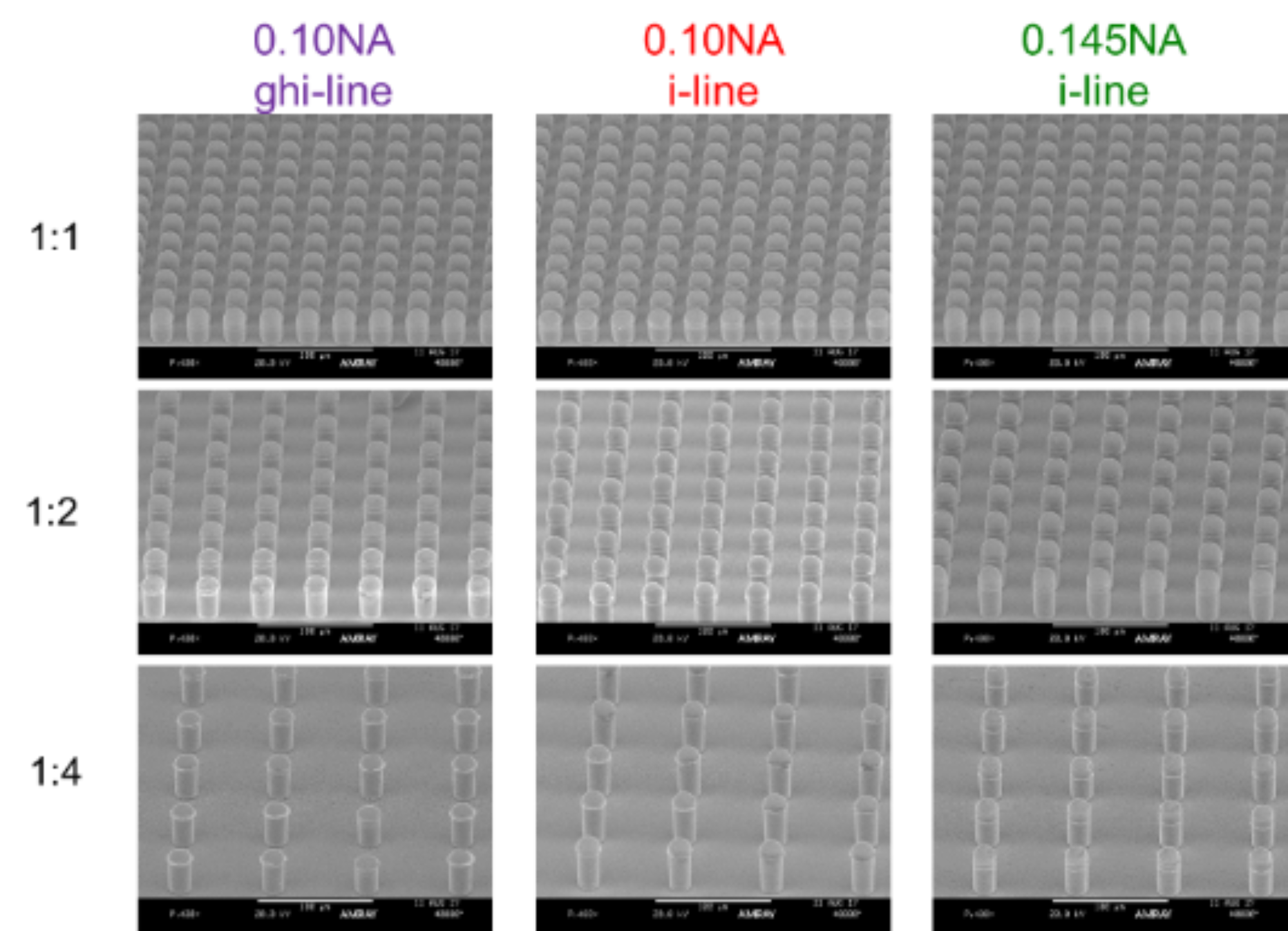
Dow’s newly-introduced chemically-amplified material is capable of film thicknesses from 30µm to 80µm by a single coating process with good uniformity. Imaging and process latitude at multiple wavelengths using a 0.1NA WLP/PLP stepper and a 0.15NA PLP stepper are demonstrated at 50µm thicknesses with emphasis on sidewall profiles and sensitivity. The power of integrating enhanced image contrast via chemical amplification and improved optical design has enabled the development of higher resolution, finer pitch back-end processing for advanced packaging technologies.