Blog Post posted on Jan 11, 2022
The ability to trace the genealogy of all the components in an electronic device has been getting more complex for decades. For many industries — automotive, defense, medical and others — the need to locate the source of a problem in near real-time is paramount to gauging the extent of that problem. The extreme case is when the issue occurs with a product that already has been distributed and used in the field. Complicating matters is the fact that the current chip shortage is pushing chip designers to second- and third-tier suppliers for their inventory.
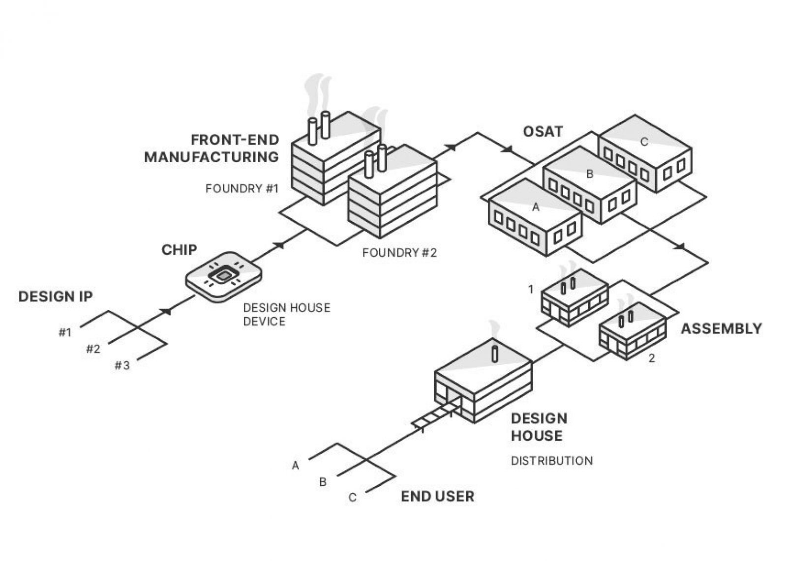
Tracking information is not easily done given the number of times material can change hands during the manufacturing life cycle. Designs can incorporate IP modules from Parties No. 1, No. 2, and No. 3 (figure 1). These designs are blended into a singular chip by the device’s Design House. This chip is then built at Front-end Foundries No. 1 or No. 2. The completed chip can be tested and partially assembled at OSAT A, B, or C. Finished assembly into a multi-chip module (MCM) or printed circuit board (PCB) can take place at Assembly House No. 1 or No. 2 (or happen at Customer A if they provide the IP for a design for a device that can be assembled by Finished Goods Maker No. 1) before it is finally sold by the Design House to the End User or Final Goods Manufacturer A, B, C, D and more for insertion in their end product, after which it is again tested before being sold to the end customer.
This is a very simplified example of how complex a supply chain can be, but it is illustrative nonetheless.
Virtual v. physical traceability
At some point in the supply chain, units receive a physical marker that enables traceability as it progresses through the remaining chain of manufacturing agents. Prior to the application of a marker, reliance on a part’s origin is a function of accounting and accurate recordkeeping. Although this seems simple enough, it is complicated by the transition of “ownership” of the chip as it moves through the supply chain.
Tracing a chip’s origin includes its transformation through multiple physical form factors. These material changes frequently include moving from a lot/wafer/die physical structure to a singulated die on a piece of tape or reel to an assembled die in a package, or in a tray, or as an inserted chip in a multi-chip module or PCB — ultimately ending with the PCB being inserted into a larger form factor, such as an automobile or a computer server. Each time the physical form factor is updated, there is a chance to break traceability in the supply chain if incoming and outgoing product labels are not meticulously documented. This is exacerbated by a lack of standardized data formats and communication frameworks throughout the supply chain. All too often, there is a gap in a unit’s back mapping. Once this occurs, any chance to trace a problem to a source is jeopardized.