White Paper posted on Mar 5, 2017
For more than 50 years the semiconductor industry has pursued Moore’s law, continuously improving device performance, reducing cost, and scaling transistor geometries down to where advanced CMOS has reached beyond the 10nm technology node. The commensurate increase in I/O count has created many challenges for device packaging which hitherto was considered low cost with simple solutions. It was once thought that old backend foundry lithography steppers could be used to address the new packaging requirements; which was true whilst the substrates remained in the traditional 300mm Silicon format. The recent unprecedented rapid growth in Fan-out Wafer Level Packaging (FOWLP) applications has introduced a more complicated landscape of process challenges, with no restriction on substrate format, where cost is the main driver and high yields are mandatory.
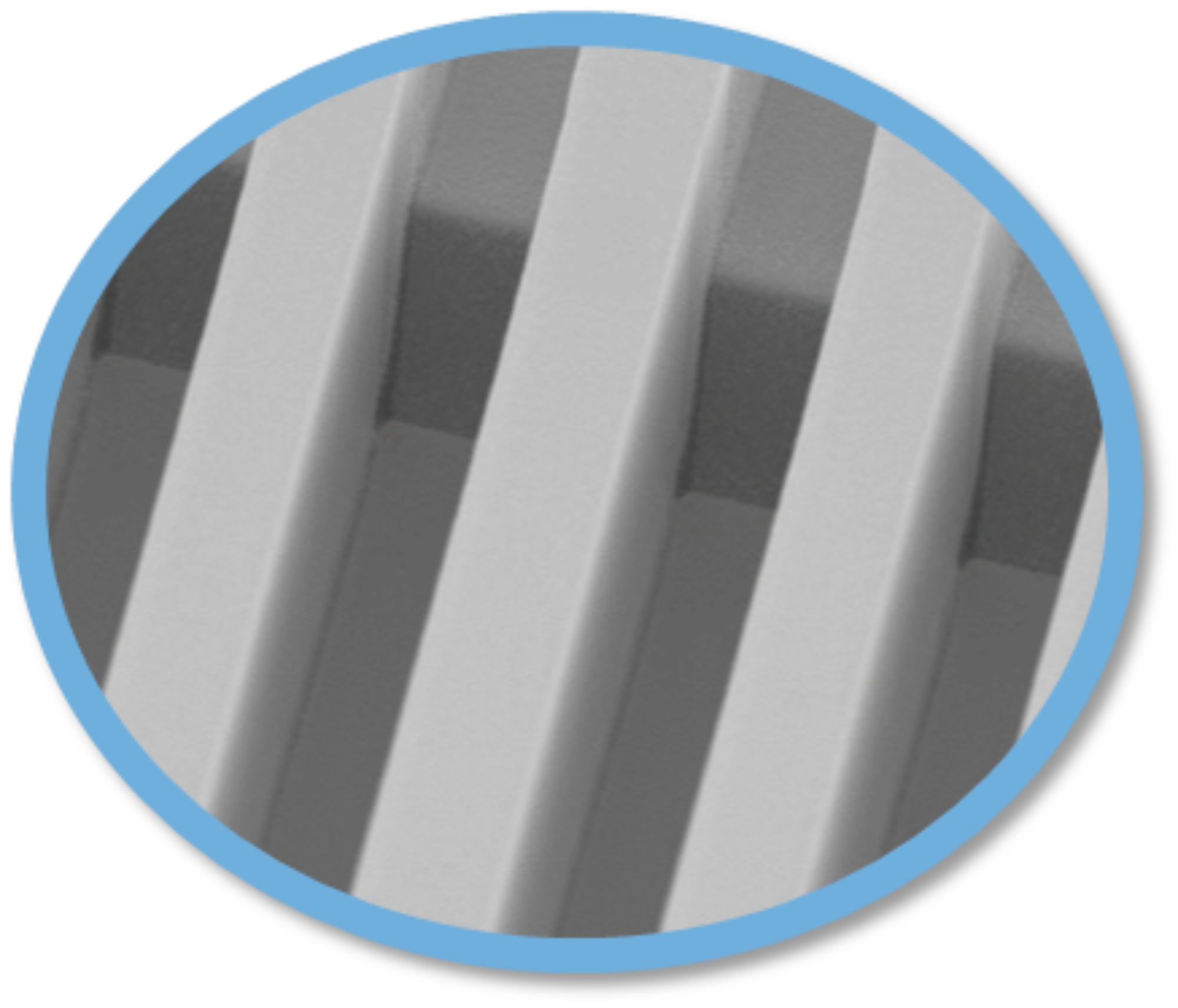
This paper discusses the lithography process challenges that have ensued from disruptive FOWLP, and more recently the paradigm shift to Fan-out Panel Level Packaging (FOPLP). The work reports on lithography solutions for CD control over topography and high aspect ratio imaging of 2µm line/space RDL. In addition, the introduction of new inspection capabilities for defects and metrology is reported for both wafers and panels. The increase in lithography productivity and cost reduction provided by FOPLP is also discussed with production examples.