
Dragonfly® G3 System
Highly configurable, automated, high speed 2D inspection and 3D metrology for inline process control in advanced packaging, specialty and front-end OQA.
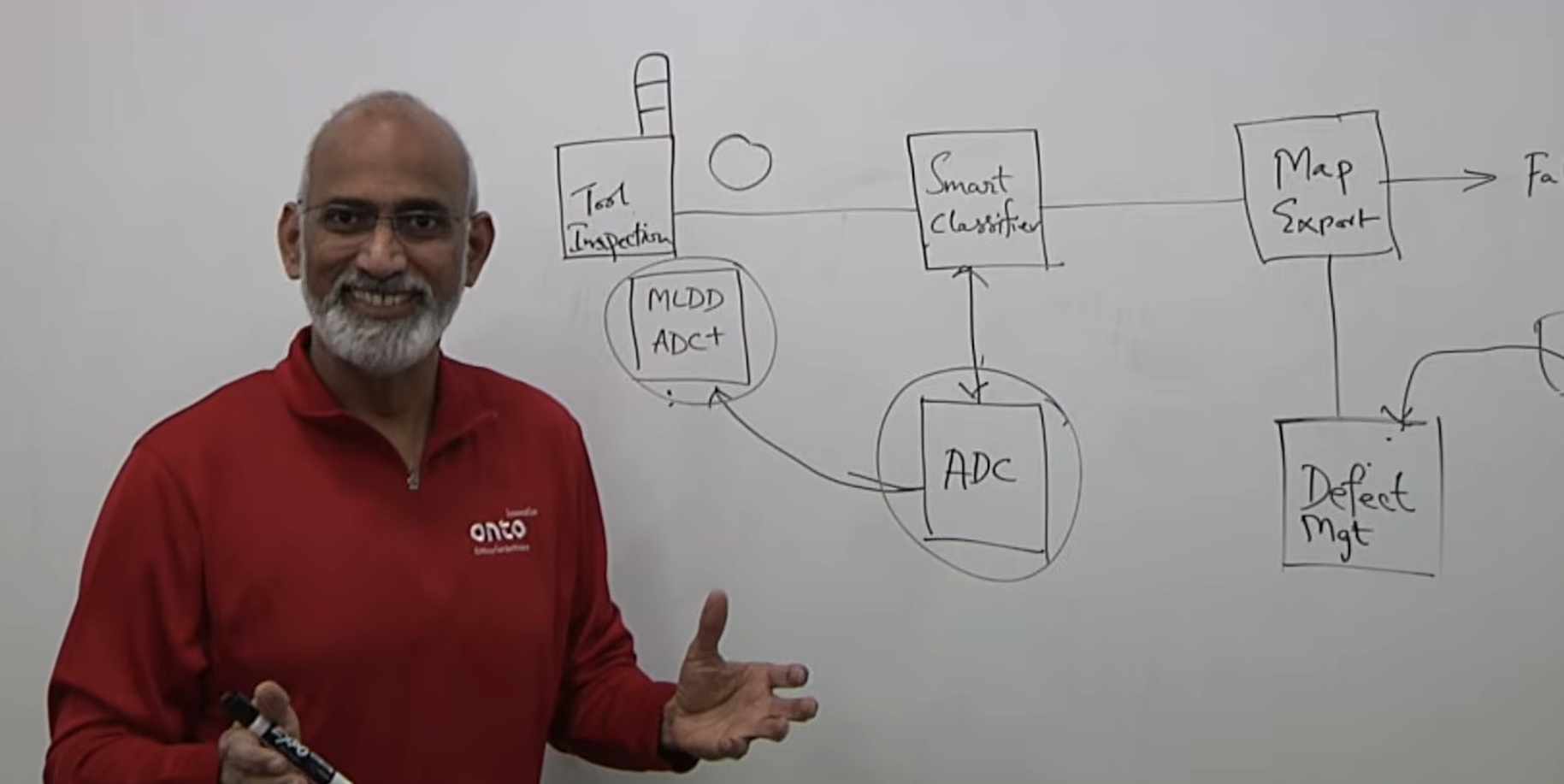
The number of defects detected through inspection is exploding at each new process node. There are now millions of defects being identified on each wafer, but only a fraction of those can cause problems.

Sept 2 — Sept 4, 2026
Onto Innovation is a proud exhibitor at SEMICON Taiwan.
The Dragonfly G5 system is engineered for inline process control of leading-edge advanced packaging technologies. As the latest generation pattern inspection system in the Dragonfly series, it delivers unparalleled accuracy in detecting submicron defects and performing high-resolution 3D measurements.
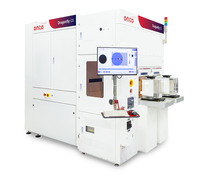
Designed to meet the demands of advanced semiconductor technologies, the Dragonfly G5 system is purpose-built to deliver high-performance, reliable inspection and metrology across complex heterogeneous integration processes. Leveraging next generation high speed line scan 2D imaging and custom-engineered objectives, the system achieves over 3X throughput improvement compared to its predecessor, with submicron sensitivity down to 150nm.
Continuing the legacy of innovation, the Dragonfly G5 system introduces a multi-angle illumination channel that significantly improves signal-to-noise ratio for faint defect detection. Combined with powerful AI-driven algorithms, it enhances both the detectability and classification of critical, yield-impacting defects–empowering fabs to maintain quality and accelerate time-to-yield.
The Dragonfly G5 system expands process control flexibility for wafer-to-wafer and die-to-wafer bonding by integrating high-speed IR imaging to detect sub-surface defects. It incorporates the latest generation of 3Di™ technology, extending bump height metrology capabilities to support next-generation microbumps essential for 3D integration. This enables additional inspection and metrology touchpoints across increasingly complex packaging architectures.


Hybrid bonding enables ultra-dense 3D memory interconnects with up to 1,000x more connections than microbumps. Achieving high yield requires stringent process control, including monitoring topography and detecting particles, cracks and voids. Measuring dishing in copper pads provides valuable insight into surface conditions. Together, these process control insights contribute to improved device reliability and performance.

As demand grows for high-performance computing (HPC) and AI-driven applications, manufacturers are turning to hybrid bonding to enable the ultra-dense 3D integration required for next-generation chip architectures. This advanced packaging technology presents significant process challenges. Surface preparation must be precisely controlled to eliminate particles, excess recess, and copper pad dishing, all of which can compromise bond quality. During pre-annealing, particle-induced gaps and wide bonding gaps can prevent proper wafer contact. Post-annealing, the formation of dielectric and metal voids introduces further risks to electrical performance and long-term reliability.

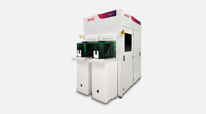
The Iris S system is a versatile platform solution for the advanced packaging and specialty market, supporting 150mm, 200mm and 300mm wafers. It provides thin and thick film, OCD and wafer bow and film stress measurements.

The IMPULSE V system helps to advance CMP processing with enhanced wavefront technology and AI-driven analytics, delivering over 2X precision improvement and faster solutions, crucial for next-gen semiconductor manufacturing demands.

The Dragonfly G5 system is engineered for inline process control of leading-edge advanced packaging technologies. As the latest generation pattern inspection system in the Dragonfly series, it delivers unparalleled accuracy in detecting submicron defects and performing high-resolution 3D measurements.

The Aspect System is a revolutionary in-line, non-destructive infrared optical critical dimension (IRCD) system measuring Z-dimension profiling of high aspect ratio structures to enable critical process control. It meets the needs of leading-edge customers with its high speed and process coverage.

As your partner for innovative solutions, we’re always here for you.
Discover how our cutting-edge semiconductor solutions are engineered to meet your most complex challenges: delivering performance, reliability and innovation where it matters most.
"*" indicates required fields
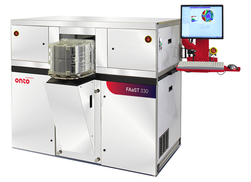
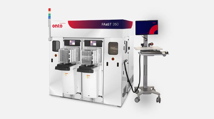
The FAaST system is a versatile, non-contact electrical metrology platform, with an option to combine micro and macro corona-Kelvin technologies together with digital surface photovoltage (SPV). It enables high-resolution dielectric and interface measurements across a wide range of dielectric materials, supporting both R&D and high volume manufacturing.
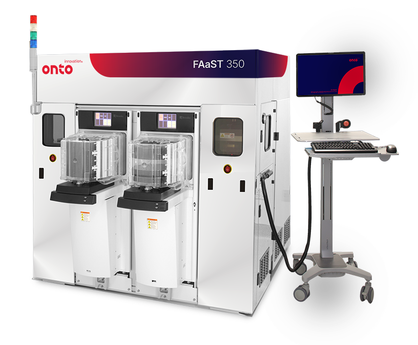
The primary application of non-contact CV metrology is monitoring dielectric properties during IC manufacturing. Unlike conventional electrical measurements, it requires no sample preparation, eliminating the need for MOS capacitor structures. This reduces metrology cost and enables fast data feedback in both R&D and manufacturing environments.
The corona-Kelvin method uses a corona discharge in air to deposit an electric charge (DQC) on the wafer surface. A vibrating Kelvin-probe then measures the resulting surface voltage (V), enabling determination of the differential capacitance (C= DQC/DV). By monitoring surface voltage in both dark and illuminated conditions, the system separates two key components: dielectric voltage (VD) and semiconductor surface potential (VSB), enabling determination of flat band voltage (VFB).
Analysis of the resulting charge-voltage data yields electrical parameters, including trap density (Dit), flat band voltage (Vfb), dielectric charge (Qtot), dielectric capacitance (CD), Equivalent Oxide Thickness (EOT), leakage current, and tunneling characteristics.
As your partner for innovative solutions, we’re always here for you.
Discover how our cutting-edge semiconductor solutions are engineered to meet your most complex challenges: delivering performance, reliability and innovation where it matters most.
"*" indicates required fields
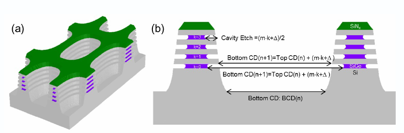
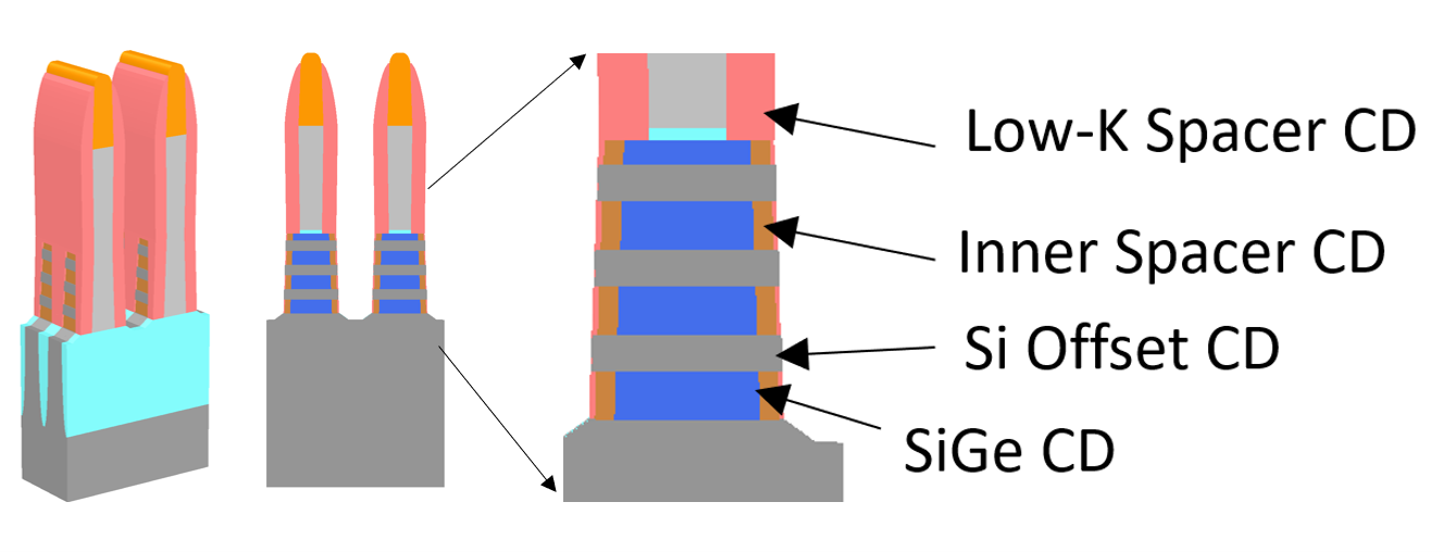
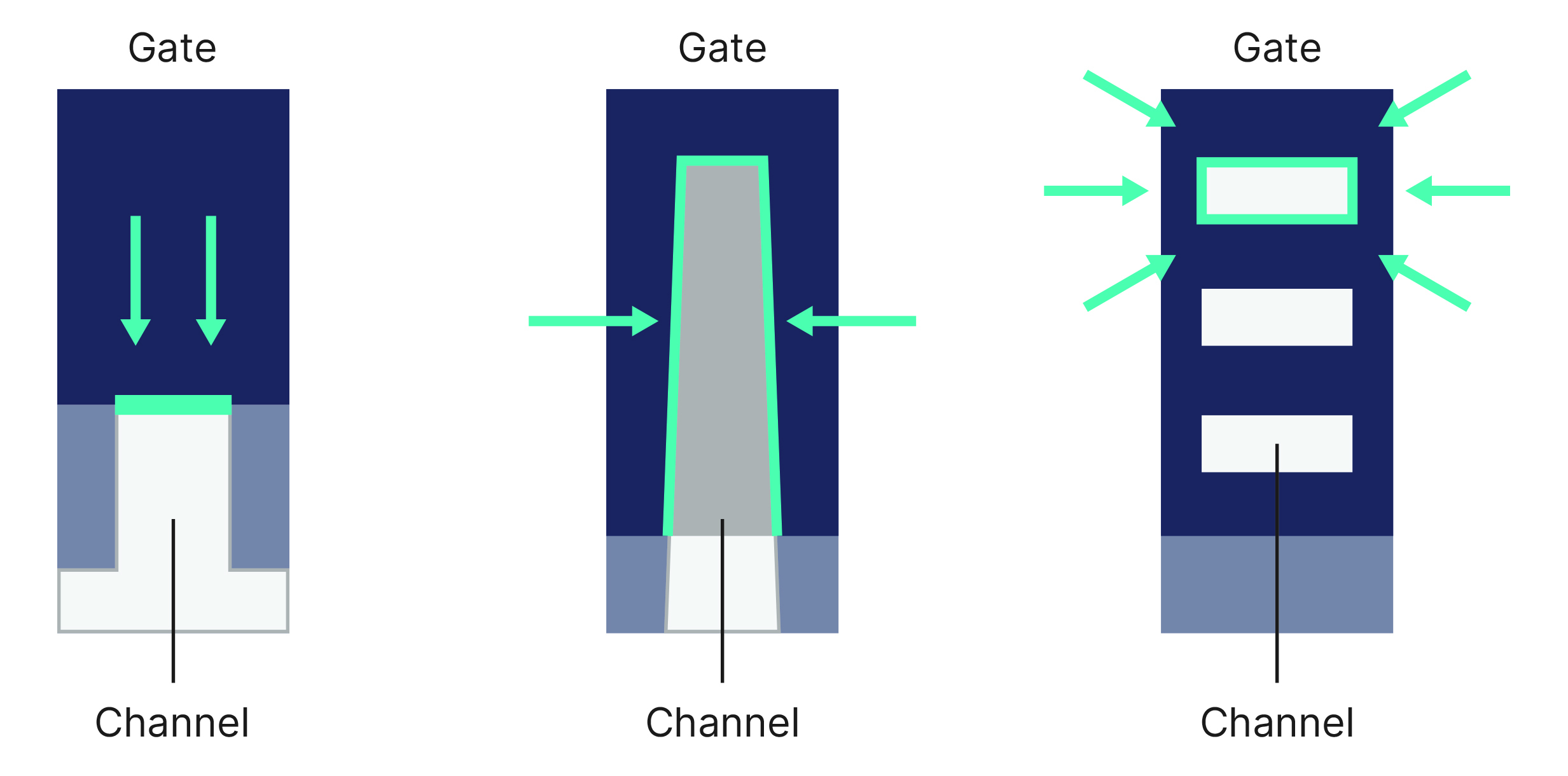
The Aspect S system is a revolutionary in-line, non-destructive model-based infrared reflectometry system that enables critical process control of high aspect ratio structures, films and epitaxial structures. It meets the needs of leading-edge customers with its high speed and process coverage.
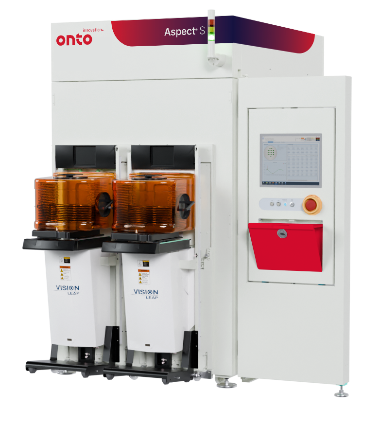
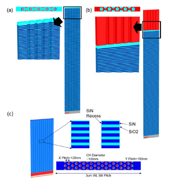
As more high aspect ratio processes are used in multiple industry segments, there are metrology needs for monitoring of related processes, including dimensions and properties of carbon film hard masks and etched 3D structures.
The Aspect S delivers high-throughput, low COO, non-contact, non-destructive measurements of dimensions and uniformity of layers and etched structures used in integrated circuit manufacturing. The small spot size makes the tool suitable for measurements of scribe line test structures as in-line process control. The unique technology and analysis capability simplifies system calibration requirements and removes the effect of substrate variations for key layer measurements.
While the software contains advanced features for measurement recipe and analysis model creation, it has a user-friendly interface and implementation that allows the fab customers to create and manage the recipe system for Aspect S tool fleets.

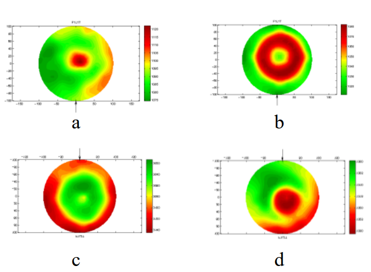
Thickness map from amorphous carbon film
As your partner for innovative solutions, we’re always here for you.
Discover how our cutting-edge semiconductor solutions are engineered to meet your most complex challenges: delivering performance, reliability and innovation where it matters most.
"*" indicates required fields
The FAaST Digital SPV system provides a fast, non-contact, and preparation-free method for full wafer imaging of contamination in silicon. High resolution maps of diffusion length and iron (Fe) concentration are generated in minutes, setting the industry standard for precision and sensitivity in Fe contamination control, reaching the E7 cm-3 range.
There is no disputing the detrimental effect of metallic contamination on the integrity of the critical gate oxide used in integrated circuits. During high temperature processing, contamination in the silicon wafer often precipitates at the Si/dielectric interface or segregates into the dielectric—both scenarios can cause premature device failure and reduced yield. As device dimensions shrink, the tolerance for contamination decreases, requiring ever-lower background levels of metals like iron (Fe). Over the past 25 years, the IC industry has reduced typical Fe concentrations by more than three orders of magnitude, yet further reduction is essential, especially for applications like CMOS image sensors.
The FAaST Digital SPV system addresses this challenge with industry-leading sensitivity and speed. It provides a fast, non-contact, and preparation-free method for full-wafer imaging of contamination. High-resolution maps of minority carrier diffusion length and Fe concentration are generated in minutes, enabling fabs to detect and control contamination at levels as low as the E7 cm⁻³ range.

Figure 1. Typical background Fe concentration in new IC Fablines (blue) and the state-of-the-art SPV detection limit (red)
As your partner for innovative solutions, we’re always here for you.
Discover how our cutting-edge semiconductor solutions are engineered to meet your most complex challenges: delivering performance, reliability and innovation where it matters most.
"*" indicates required fields
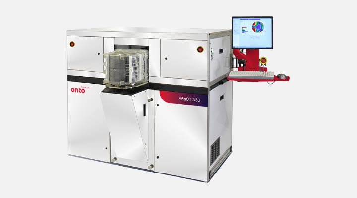
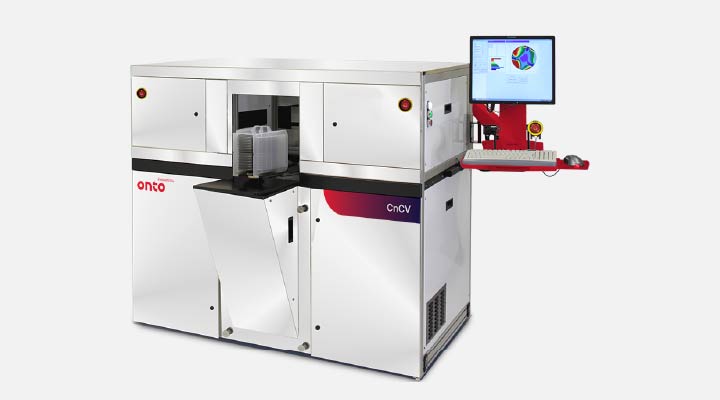
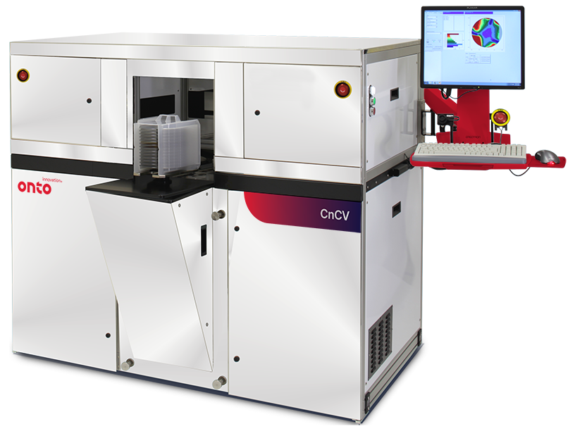
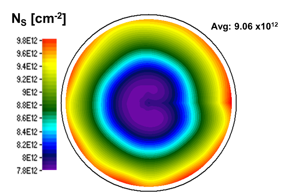
The CnCV system enables wafer-level characterization of WBG materials without test device fabrication, reducing time and cost. As a mercury-free alternative to MCV, it eliminates contamination concerns. The enhanced Kinetic CV mode with UV-assisted corona charge neutralization achieves high throughput and precision for fast, reliable process control.
The CnCV system utilizes a novel constant surface potential corona charging, which enables the precision required over a large voltage range. The patented technology includes charge- and photo-assisted modes, especially suited for speed and precision on WBG materials and structures, including SiC, Ga2O3, GaN, and AlGaN/GaN HEMT. Additionally, Corona-Kelvin characterization includes electrical properties of dielectrics and interfaces of films on SiC and GaN epi layers. An automated top-side edge contact (TSEC) is also available enabling characterization of WBG on insulating/semi-insulating substrates. Automated bias-temperature stress (BTS) measurements are also available with the CnCV system, providing a fast, noncontact way to quantify the reliability of passivated SiC and GaN.
Beyond typical CV type parameters, the full wafer corona approach allows for QUAD (quality, uniformity, and defect) mapping. The electrical defect imaging, QUAD-EDI, mode is especially designed for SiC. It provides a unique means for quick screening of epi electrical defectivity enabling improvement in device yield prediction.

Figure 1. QUAD-EDI Map on final metallized device wafer after Merged Schottky PiN diode fabrication identifying failed dies.
As your partner for innovative solutions, we’re always here for you.
Discover how our cutting-edge semiconductor solutions are engineered to meet your most complex challenges: delivering performance, reliability and innovation where it matters most.
"*" indicates required fields
A suite of OCD modeling software and computing hardware that enables the full capability and connectivity across all Onto OCD and thin film metrology systems, including Atlas, Aspect, Iris and IMPULSE systems.
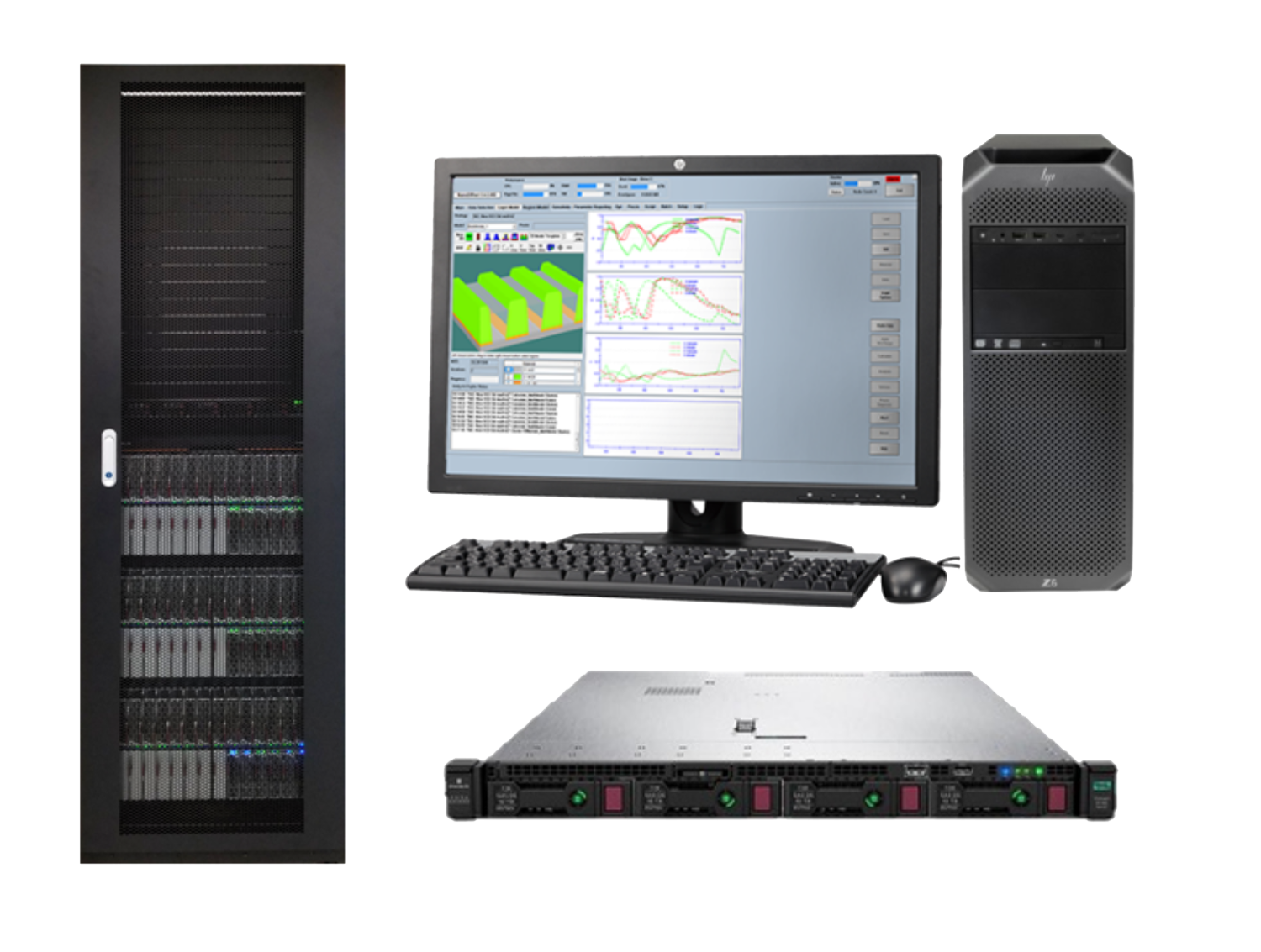
Onto Innovation’s OCD technology offers powerful modeling and computing packages to support various phases of film and OCD measurement setup, data management, and fleet management. These capabilities include model building, runtime data analysis, system calibration, data analytics, data connectivity and management, spectrum management and fleet matching.
Onto OCD solutions consist of several modeling and computing components, including Ai Diffract™ modeling software, runtime onboard computer, offline modeler, offline model building clusters, and recipe & data management server. Each component seamlessly extends OCD capabilities to Onto’s standalone and integrated metrology systems, providing end-to-end capabilities from offline recipe support and development to fab-wide networking and connectivity for easy fleet management.
Ai Diffract software is a powerful modeling, visualization and analysis software with an intuitive 3D modeling interface to simplify the building and visualization of today’s most complex semiconductor devices. It offers OCD modeling and advanced machine learning capabilities, next-generation real-time regression, offline sensitivity analysis tools and comprehensive GUI and structure input for true multi-variant modeling. Ai Diffract software’s proprietary fitting algorithms enable fast and accurate calculations for signal processing, helping ensure high fidelity model-based measurements. Automation features for spectral fitting, recipe optimization, and sensitivity analysis offer great user productivity. The first-in-market AI-guided engine synergizes physics-based modeling and machine learning to deliver the most robust solution with quick time to solution.
Ai Diffract Modeler is the offline analytical engine that allows users to create and edit recipes offline. It supports multiple users and can connect to Ai Diffract cluster for high intensity computing.
Ai Diffract Onboard is the on-tool runtime engine that maximizes tool throughput for complex use cases. It ensures rapid analysis without interfering with system operation or impacting throughput.
Ai Diffract Cluster is an enterprise scale computing server deployed for offline recipe development or in-line real-time regression. Optimized to support the workload of Ai Diffract software analysis, it scales based on fleet size, recipe numbers, and computing intensity.
Recipe Distribution Server (RDS) / Nexus Servers is a fab-wide networking and server system for fleet management and connectivity. RDS/Nexus servers provide connectivity and support to Ai Diffract recipe management and distribution, data/spectrum feed-forward and feedback, spectrum management, and fleet management.


As your partner for innovative solutions, we’re always here for you.
Discover how our cutting-edge semiconductor solutions are engineered to meet your most complex challenges: delivering performance, reliability and innovation where it matters most.
"*" indicates required fields