

Mid-infrared ellipsometry for optical critical dimension metrology
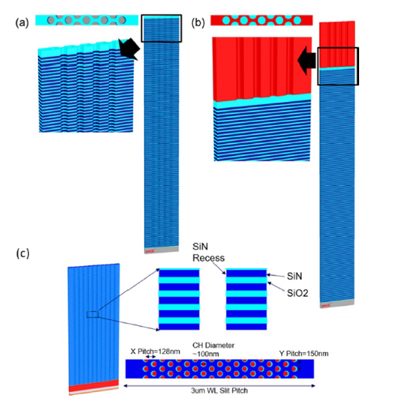
Mid-infrared ellipsometry offers a powerful approach for non-destructive optical critical dimension (OCD) metrology in advanced semiconductor manufacturing. This technique supports in-line measurements of high aspect ratio structures, such as those found in 3D NAND memory devices. The incorporation of quantum cascade lasers and fast phase modulation allows rapid acquisition of Mueller matrix elements with high spatial resolution and sub- Å precision. Material-specific absorption in the mid-infrared range allows depth-resolved profiling of device structures, overcoming the limitations of conventional OCD. Rigorous coupled wave analysis is used to extract structural parameters from the measured spectra. Agreement with destructive reference metrology has been demonstrated on a variety of structures. The ability to measure multiple Mueller elements further enhances characterization of complex geometries, making mid-infrared ellipsometry a valuable tool for process control in semiconductor fabrication.
This article may be downloaded for personal use only. Any other use requires prior permission of the author and AIP Publishing. This article appeared in Journal of Applied Physics (Vol.139, Issue 7) and may be found at https://doi.org/10.1063/5.0310009
DOI: 10.1063/5.0310009

You Have a Challenge? Let’s talk.
We’d love to connect with you.
Looking to learn more about our innovative solutions and capabilities? Our team of experts is ready to assist you. Reach out today and let’s starts a conversation about how we can help you achieve your goals.
Let’s Talk
"*" indicates required fields