

A Review of Recent Technological Advancements in Corona Noncontact Metrology Tools, CnCV, for Industrial WBG Wafer Testing and Electrical Defect Related Yield Prediction
Abstract
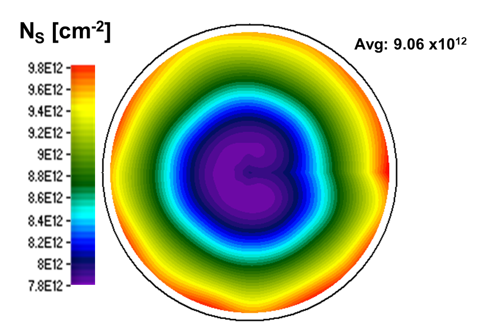
In this review we discuss two recent CnCV metrology advancements, namely: 1. enhancement of throughput and 2. use of electrical defect mapping for yield prediction. Novel 10x faster measurements of critical WBG semiconductor electrical parameters are based on the discovery of a linear UV radiation induced electrical charge biasing. Example results for an AlGaN/GaN HEMT structure illustrate wafer uniformity mapping reduced from hours to minutes and enabling the prediction of the useful wafer area. The second development on SiC device yield was realized as a joint project with Nexperia and Fraunhofer IISB in Germany [2]. The project took advantage of the unique electrical defect mapping capability of the QUAD (Quality, Uniformity and Defect) technique in CnCV tools. Macro and micro-scale QUAD mapping applied to a merged PiN Schottky (MPS) diode manufacturing process correlated QUAD bin map results with failed dies identifying the culprit epi-layer and process induced defects. This development paves a realistic path for meeting the demand for more advanced electrical defect detection and improving device yield prediction.

You Have a Challenge? Let’s talk.
We’d love to connect with you.
Looking to learn more about our innovative solutions and capabilities? Our team of experts is ready to assist you. Reach out today and let’s starts a conversation about how we can help you achieve your goals.
Let’s Talk
"*" indicates required fields