
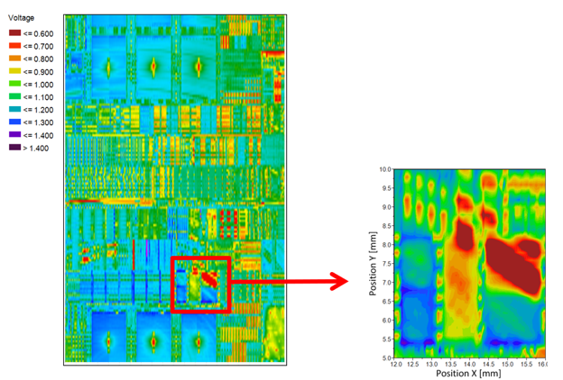

Electric vehicles, fast-charging infrastructure, renewable energy systems, and industrial power conversion are redefining what power semiconductors need to deliver: higher voltages, higher power densities, faster switching, and longer lifetimes. To meet these demands, manufacturers are increasingly turning to wide-bandgap materials like silicon carbide (SiC) and gallium nitride (GaN).
SiC has become the material of choice for high-voltage applications such as traction inverters, onboard chargers, and motor drives, while GaN is widely adopted in fast-charging and high-frequency power devices. As these end products scale in volume and performance, the pressure on semiconductor manufacturing to deliver consistent yield and reliability continues to mount.
At the same time, manufacturers are undergoing critical transitions in wafer size. SiC production has moved from 150mm to 200mm wafers for high-volume manufacturing (HVM), with 300mm substrates for advanced packaging applications in early-stage development and limited demonstration. GaN, which historically has been manufactured on 200mm wafers, is also expanding into 300mm GaN-on-silicon. These transitions are essential for cost reduction, but they also introduce significant wafer handling, inspection, metrology, and yield challenges.
What conventional inspection misses
A defining characteristic of many SiC power devices is that they conduct vertically, from the front side of the wafer to the backside. This architecture fundamentally changes how defects impact performance and reliability.
In vertically conducting devices, crystalline defects that originate in the substrate or propagate through the epitaxial layers can directly create leakage paths, increase resistance, or cause catastrophic device failure. Some of these defects may be electrically benign at low stress levels, only to become yield-limiting once devices are operated at high voltage in the field.
This introduces a critical manufacturing challenge: not all defects are equal, and not all defects that matter are visible with traditional inspection techniques.
Traditional surface-based optical inspection is effective for detecting particles and some surface features, but it struggles to detect subsurface or crystalline defects that directly impact electrical behavior in wide-bandgap materials. As wafer sizes grow, these limitations become more pronounced.
Compounding the problem, many inspection systems rely on spinning-wafer architectures, which can introduce center-to-edge sensitivity variation, particularly as wafer sizes scale to 200mm and 300mm. This loss of uniform sensitivity becomes increasingly problematic at 200mm and even more so at 300mm, exactly where manufacturers can least afford blind spots.
For manufacturers scaling expensive SiC wafers, detecting defects is no longer enough. Understanding which defects are likely to impact yield and reliability is what matters most.
Photoluminescence (PL) inspection addresses this gap by enabling high-sensitivity, full-wafer detection of defect-related variations that are otherwise difficult to capture with conventional inspection approaches. When crystalline defects are present, they alter how the material emits light under excitation. In this way, manufacturers can use PL to reveal defect-related signatures and regions associated with performance variation, insights that are not visible with purely surface-based inspection techniques.

Fig. 1: Examples of defects identified by photoluminescence technology.
This capability is especially valuable for wide-bandgap materials where crystalline quality is tightly linked to electrical performance. PL inspection provides a powerful way to detect subsurface defects early in the process before device fabrication adds cost and complexity. High-sensitivity PL systems equipped with advanced optical designs and multi-channel detection provide the sensitivity needed to detect these subtle defect signatures across the full wafer.
As wafer sizes increase, inspection architectures must scale with them. XY stage inspection platforms, which scan the wafer without spinning it, maintain consistent sensitivity from the center to the edge of the wafer. This approach avoids the sensitivity roll-off inherent in spinning systems and provides a scalable and uniform inspection approach for larger wafers.
Equally important, modern PL inspection tools are designed with wafer-size flexibility in mind, enabling manufacturers to support current production needs while preparing for future substrate transitions without retooling their inspection strategy. While these advancements improve inspection capability, they do not fully address the need to connect defect data across the manufacturing flow.
Advanced manufacturers increasingly recognize that inspection tools cannot operate in isolation. Real value comes from integrating inspection, characterization, and data analysis into a coherent yield-learning strategy. This requires consistent, scalable correlation across optical, electrical, and process domains.
One example is sub-defect or root-cause defect mapping, where bare substrates are inspected first to establish an initial defect baseline. The same wafers are then re-inspected after epitaxial growth to identify which substrate defects propagate into the epi layers. This comparison enables manufacturers to distinguish between latent defects and defects directly threatening yield.
While traditional PL inspection can effectively detect and classify crystalline defects, it cannot determine which of these are electrically active and contribute to device failure. In contrast, non-contact electrical metrology based on corona-charged surface voltage mapping directly identifies and images electrically active defects linked to leakage currents and breakdown behavior in finished devices.
Combining PL and electrical defect imaging enables the correlation of specific epitaxial defect types with their wafer-scale spatial distribution and electrical activity, while also tracking substrate defects that persist through epitaxial growth. This provides a comprehensive view of defect impact on device performance, yield, and reliability.
By connecting defect location, type, and electrical activity, manufacturers can move beyond defect detection and begin assessing the true impact of individual defects on device performance and yield.
True defect intelligence
Beyond technical complexity, the economics of compound semiconductor manufacturing further amplify these challenges.
The economic stakes of compound semiconductor devices are high. A 200mm silicon wafer may cost a few hundred dollars, but a 200mm SiC wafer can cost an order of magnitude more than silicon wafers. Costs rise even further at larger diameters. Scrapping wafers late in the process or shipping marginal devices that fail in the field is no longer acceptable.
By detecting critical defects earlier, correlating optical and electrical data, and accelerating root-cause analysis, integrated inspection strategies help manufacturers protect yield, improve process learning, and confidently scale production.
As end-market products continue to push performance boundaries, power semiconductor manufacturing must evolve in parallel. Vertically conducting wide-bandgap devices demand inspection solutions that go beyond surface detection and deliver true defect intelligence.
As a result, inspection strategies must evolve from isolated detection steps to integrated, data-driven approaches that connect defect detection with process insight. Photoluminescence inspection, when combined with scalable system architectures, electrical characterization, and integrated data analysis, provides manufacturers with the tools needed to meet these challenges.
Increasingly, the value of these capabilities lies not in any single technique, but in how they are brought together within a unified inspection and analysis ecosystem, an approach that depends on tightly integrated system architectures, multi-modal data correlation, and scalable workflows to convert defect data into actionable process insight. For next-generation power semiconductors, this integrated approach is not just beneficial, it is becoming essential.
Jason Lin is director of product marketing at Onto Innovation.
You Have a Challenge? Let’s talk.
We’d love to connect with you.
Looking to learn more about our innovative solutions and capabilities? Our team of experts is ready to assist you. Reach out today and let’s starts a conversation about how we can help you achieve your goals.
Let’s Talk
"*" indicates required fields
From consumer products to industrial applications, augmented reality (AR)/mixed reality (MR) technology is one of the most innovative interactive technologies on the market today. By overlaying digital information onto the physical world, AR/MR technology improves how people see, understand, and interact with their environment in real time. The industrial applications alone are cause for celebration, whether this technology is being used for training, assembly, or troubleshooting.
Be that as it may, one of the most significant challenges facing AR/MR lies in manufacturing the photonic components that control how light is generated, diffracted, guided, and delivered to the human eye.
An AR display usually consists of a light engine and an optical combiner. The light engine serves as a display image source, while the combiner delivers the displayed images to the viewer’s eye and transmits environment light (Figure 1). Surface relief grating (SRG) waveguides play a role in these optical combiners by coupling display light into, expanding it within, and diffracting it out of a transparent substrate toward the eye of the intended viewer. This component must deliver precise diffraction behavior while remaining transparent, lightweight, and scalable for high-volume manufacturing (HVM).
Balancing optical performance and manufacturability, however, places significant demands on fabrication and process control. Faced with this obstacle, device makers require solutions capable of addressing any negative impacts to launch timelines, unit costs, and OEM qualification.

Figure 1. Diagram of SRG waveguide-based AR display.
In this article we will discuss ways SRG manufacturers can address these challenges with an integrated process control solution tailored for the HVM of SRG. The solution combines optical critical dimension (OCD) metrology for the critical parameters of SRG such as grating depth, slanted angle, and periods; picosecond ultrasonic technology for the metal film thickness measurement; image‑based overlay (IBO) for precise overlay control in HVM specialty devices; and an automated optical inspection for defects integrated throughout the entire manufacturing process.
With these tools combined in a closed‑loop process control strategy, manufacturers have a framework that enables the consistent manufacturing of full‑color SRG waveguides capable of meeting the stringent optical and mechanical requirements of next‑generation AR/MR devices.
Navigating the Ramp to HVM
By coupling light into and out of a transparent substrate through precisely engineered diffraction gratings, SRG waveguides can deliver wide field‑of‑view, high brightness, and compact form factors. Unfortunately, manufacturers of SRG waveguides must face a host of challenges arising from multi‑layer and often double‑sided fabrication, with sub‑100nm alignment tolerances across large‑area substrates, if they hope to transition to HVM. The impact of these challenges, however, only grows as the manufacturing process goes on, increasing yield variability and making it difficult for makers of SRG components to meet the requirements expected by tier-one AR/MR customers.
To begin with, let’s turn to grating geometry. Manufacturers must control for period, depth, and slanted angle to ensure diffraction efficiency and uniformity across the field. Additionally, makers of these components must maintain proper thickness uniformity to avoid phase errors and color shifts; as such, thin‑film processes like mask deposition and etching must maintain exceptional thickness uniformity. Third, manufacturers must also maintain overlay accuracy between lithography steps, and they must do so within a fraction of the design tolerance to preserve red, green, and blue (RGB) multi‑period grating registration and double‑sided alignment. Finally, defect control is essential in the manufacturing process. After all, particles, scratches, and etch anomalies can cause scattering, reduce optical efficiency, and degrade image quality. Not surprisingly, the manufacturing process features a number of consequential steps (Figure 2).
In many cases, the process begins with the deposition of a chromium (Cr) hard mask on a SiO₂ substrate, followed by spin coating a resist layer. For master fabrication, electron beam lithography or deep ultraviolet lithography is used to pattern the grating structure. The resist pattern is then transferred to the Cr layer using a dry etching process, after which the residual resist is removed, leaving the Cr layer to serve as an etching mask for reactive-ion beam etching (RIBE). During RIBE, ionized argon beams are directed toward the substrate at an oblique angle to form the slanted grating profile. Once the target etch depth is achieved, the Cr layer is removed by chemical wet etching.
For HVM, the fabricated master grating is replicated using nanoimprint lithography (NIL) production due to its low cost and high throughput. In this process, the master pattern is first transferred into a polymer film to form a soft working stamp, which is then used to imprint a high refractive index (RI) resist layer. After imprinting, the pattern in the high-RI resist retains the same orientation as the original NIL template.

Figure 2. Basic flow in the manufacturing process of the surface relief grating waveguide.
These manufacturing challenges—spanning nanoscale grating fidelity, thin-film uniformity, overlay accuracy, and defect control—are tightly coupled and cannot be addressed in isolation without compromising yield or optical performance. Achieving stable, HVM requires coordinated visibility into each step of the SRG process. As it stands, makers of waveguide components rely on isolated measurements that diagnose symptoms without revealing root causes. In contrast, an integrated, closed-loop approach connects thickness, CD, overlay, and defect data, allowing engineers to correct process drift before it impacts customer-visible performance. By applying integrated metal film metrology, OCD measurement, image-based overlay control, and advanced defect inspection to the process flow, manufacturers are able to establish control and consistent SRG waveguide manufacturing, improving yield during ramp and reducing qualification cycle times, an important win for manufacturers ramping up HVM.
Tackling Thickness Non-Uniformity
As part of this integrated process control framework, thickness uniformity is a critical variable to address. In SRG manufacturing, thickness and uniformity must be precisely measured and controlled as it directly impacts downstream etch behavior, grating geometry, and ultimately optical performance. Uncontrolled metal film thickness is a frequent root cause of profile distortion and yield loss in SRG waveguides. When combined with CD, overlay, and defect control, the ability to measure metal thickness enables full process visibility across SRG manufacturing.
After deposition, the hard mask must be thick enough to remain intact throughout the entire etching process without being prematurely etched through. However, excessive thickness can distort the etched sidewall profile. Moreover, non-uniform thickness across the wafer can lead to variations in etch depth and grating tilt angle. This degrades diffraction efficiency and wavefront quality.

Figure 3. Cr and Al spectra and measurement result mapping.
To measure thickness, makers of SRG components can use an inline metal film metrology tool with picosecond ultrasonic technology. This tool offers rapid and precise determination of Al/Cr thickness across different substrates, delivering within wafer uniformity characterization that facilitates the early identification of process deviations.
In our demonstrations, we used an inline metal film metrology tool to gather data. The metrology system can measure metal film thickness across the wafer and with repeatable, stable precision over time, making it suitable for tight process control in high-volume SRG waveguide manufacturing. In production demonstrations, the results showed high-precision metal film thickness measurements with strong wafer-level uniformity and repeatability across representative substrates and multilayer film stacks (Figure 3). In addition, the metal film metrology tool achieved outstanding dynamic and static stability, thereby ensuring compliance with the rigorous demands of advanced process control as shown in Table 1. This level of control offered by the inline metal film metrology tool directly reduces grating profile drift between lots, lowering rework rates and preventing late-stage optical fallout during customer acceptance testing.
| Film information | Wafer Uniformity | Repeatability(1σ) | |||
| Average | Stdev | 1 σ | Static | Dynamic | |
| Si/Al3000Å | 2676.7 | 53.4 | 2.00% | 0.03% | 0.01% |
| Glass/Resin5000Å/Al3000Å | 2706.8 | 52.2 | 1.93% | 0.10% | 0.04% |
| Si/Cr220Å | 215.1 | 3.6 | 1.66% | 0.04% | 0.00% |
| Glass/TiO2600Å/Cr220Å | 223.2 | 4.5 | 1.99% | 0.15% | 0.10% |
Table 1. Cr and Al wafer uniformity and repeatability.
Meeting Tight Design Tolerances with OCD Metrology
In the fabrication of SRG waveguides, optical performance is highly sensitive to nanometer scale variations in grating period, depth, sidewall angle, and fill factor. Manufacturers of these components must adhere to the extremely tight design tolerances required for target coupling efficiency, polarization control, and chromatic uniformity throughout the manufacturing process.
To accomplish this, manufacturers can deploy OCD metrology based on rigorous coupled wave analysis (RCWA) to continuously monitor grating depth, CD, and sidewall angle before optical deviations propagate downstream. In demonstrations, we used an OCD metrology system based on RCWA to decode light scattering signals and simultaneously extract grating parameters across the entire wafer. Two types of SRGs were targeted: blazed SRGs and binary SRGs. Binary SRGs use a two-level stepped profile for phase or polarization control, and blazed SRGs use a slanted or ramped profile to efficiently direct light into a preferred direction.
Using OCD metrology, measurements of key parameters showed excellent agreement with reference metrology in representative SRG structures, confirming the suitability of OCD metrology for process control in SRG manufacturing. This stability enables tighter process windows and allows manufacturers to run closer to design limits without sacrificing yield, a critical need in situations where OEM specifications leave little margin.


Figure 4 .(a) OCD mode of blazed SRGs, matching with reference and dynamic performance. (b) OCD mode of binary SRGs, matching with reference and dynamic performance.
Preserving Full-Color Performance Through Precise Overlay
For manufacturers, maintaining overlay accuracy between successive patterning steps is a critical determinant of optical performance. Even small misalignments can cause coupling efficiency loss, field-of-view distortion, polarization imbalance, and chromatic aberrations.
Although a single SRG is typically formed in one patterning step, waveguide processes often require multiple patterning steps or the integration of several functional gratings on the same substrate. Representative cases include separate in-coupling and out-coupling gratings, multiwavelength gratings for full color operation, where red, green, and blue gratings of different periods are overlaid in the same location via multiple lithography or multiple nanoimprint patterning steps performed on both sides of the substrate, and precise registration with other micro-optical structures. These scenarios have stringent requirements. As such, overlay control at the submicron level is needed to preserve designed optical characteristics. Meeting these stringent alignment requirements in SRG waveguide architectures necessitates precise, wafer-scale overlay metrology. IBO techniques provide component makers with the capability to directly measure and control cross-layer and double-sided alignment in transparent substrates.

Figure 5. Bar-in-bar (BIB) and overlay fingerprint.
For our demonstration we used IBO technology enabling cross-layer and double-sided alignment in transparent waveguide substrates by matching grating pattern features. Using a bar-in-bar (BIB) mark for full map overlay measurement, demonstration measurements showed that the system achieved a precision of 0.26nm (X) and 0.18nm (Y) at 3σ (Figure 5). The measured tool-induced shift (TIS) was -2.63nm (X) and -0.71nm (Y), with corresponding 3σ TIS values of 0.62nm and 0.81nm, respectively (Table 2). Based on the industry standard 3σ definition, the resulting total measurement uncertainty (TMU) was 0.83nm in the X direction and 0.92nm in the Y direction. These results demonstrate that the overlay platform delivers sub-nanometer overlay capability and provides sufficient margin for the alignment requirements of high precision, full-color SRG waveguide manufacturing. In addition, the system provides correction parameters that can be directly applied to the lithography tool to compensate for systematic overlay errors.
| RG X Avg (nm) | RG Y Avg (nm) | RG X 3S (nm) | RG Y 3S (nm) | TIS X Avg (nm) | TIS Y AVG (nm) | TIS 3σ X (nm) | TIS 3σ Y (nm) |
| -71.8 | 36.0 | 0.3 | 0.2 | -2.6 | -0.7 | 0.6 | 0.8 |
Table 2. Overlay measurement statistics.
Detecting Submicron Defects
Defect inspection is critical to the manufacturing of SRG waveguides. Due to the unique nanoscale periodic structures and the optical sensitivity of SRG waveguides, even minor defects can lead to reduced diffraction efficiency, increased stray light, image non-uniformity, and other issues. As a result, defect inspection should be integrated throughout the entire SRG manufacturing process. In the mass production of SRG waveguides using NIL, manufacturers are enabled to detect organic defects from the photo resist, cleaning chemical residues, and high index resin which would normally escape detection under conventional brightfield or darkfield illumination schemes. In HVM undetected submicron organic defects can propagate across replicated stamps, turning a localized issue into a systemic yield problem.
The automated defect inspection system we employed provides fast and reliable inspection for submicron defects and the option to accurately measure 2D and 3D metrology features. Equipped with multiple illumination technologies, the inspection system is capable of capturing organic defects at or below 1µm. Standard optical inspection struggles with features at this size, opening the door to defect contamination that would otherwise be invisible but detrimental.
The Continued Evolution of AR/MR Technology
With the advent of mass production and declining costs of SRG waveguides, the coming years are poised to mark a transformative phase for AR/MR technology. This article presents an approach for full process control for the HVM of SRG waveguides, encompassing metal film metrology, OCD measurements of grating parameters, overlay alignment verification, and defect inspection—spanning from incoming substrate qualification to the validation of the final product.
The process‑control challenges discussed in this article extend across a broad class of AR/MR optical architectures, diffractive and meta-optical devices, and other nano-patterned optics manufactured at scale. Beyond SRG waveguides, the same process-control capabilities extend across a wide range of optical and photonic manufacturing applications, including other AR/MR waveguide architectures such as volume holographic and multi-level diffractive waveguides, as well as diffractive optical elements and meta-optics that rely on sub-wavelength pattern fidelity and precise depth control. These applications overlap strongly with optical thin-film stacks and functional coatings, micro-display manufacturing, and advanced optical and silicon-photonics packaging, all of which demand tight control of CD, overlay, film uniformity, and defectivity to reach HVM.
For manufacturers evaluating their next waveguide ramp, the key question is no longer whether SRG waveguides can meet optical targets, but whether their process control strategy can meet OEM schedules, cost models, and yield expectations at the same time. With the right integration of tools on hand, they can.
Biography
Alex Hong is a Senior Field Application Engineer at Onto Innovation, specializing in metal film metrology for semiconductor manufacturing, with additional expertise in optical critical dimension (OCD) applications.
The author would like to thank the rest of the team who worked on this article, including Onto Innovation’s Huayuan Li, Charles Zhang, Yuhang Lin, and Johnny Mu, along with Xiongwei Wang and Chenglong Jia of Sunny Optical Oulai Micro-Nano Optics (Shanghai) Co., Ltd.
You Have a Challenge? Let’s talk.
We’d love to connect with you.
Looking to learn more about our innovative solutions and capabilities? Our team of experts is ready to assist you. Reach out today and let’s starts a conversation about how we can help you achieve your goals.
Let’s Talk
"*" indicates required fields

You Have a Challenge? Let’s talk.
We’d love to connect with you.
Looking to learn more about our innovative solutions and capabilities? Our team of experts is ready to assist you. Reach out today and let’s starts a conversation about how we can help you achieve your goals.
Let’s Talk
"*" indicates required fields
Every day, consumers rely on an invisible network of specialty semiconductor devices without realizing it. The smartphone in your pocket is a good place to start. It knows when you rotate the screen thanks to MEMS sensors, and its camera delivers crisp images through advanced CMOS image sensors. Meanwhile, fast charging technology, wireless connectivity, facial recognition, and high-frequency communications all depend on specialty power devices, radio frequency (RF) filters, and photonic technologies working seamlessly behind the scenes.
However, success in every specialty device category hinges on advanced process control solutions capable of ensuring what matters most is tightly understood and controlled. This may be shape, thickness, uniformity, defects, or material properties. And it all must be done at low cost of ownership while maintaining the throughput needed for high-volume manufacturing (HVM). For device manufacturers, failure to meet requirements doesn’t just increase process complexity, it directly translates into longer ramps, missed customer commitments, and higher cost per device.
As we explored in the first two parts of this of our Specialty Surge series, these unsung heroes of modern electronics are rapidly scaling in complexity and volume, causing headaches for device manufacturers. In this final blog, we’ll turn our attention to the strategies manufacturers can employ to make that pain go away. From advanced metrology to inspection and data-rich feedback for process control, we’ll explore the capabilities enabling specialty devices to deliver the performance consumers expect at the scale manufacturers want.
Challenges Revisited
Before we go any further, let’s recap the challenges specialty device manufacturers face, separated by device type. We’ll begin with microelectromechanical systems, a.k.a. MEMS.
MEMS – MEMS include a variety of device types, including pressure sensors, gyroscopes, accelerometers, microphones, and surface acoustic wave (SAW)/bulk acoustic wave (BAW) radio frequency MEMS. These devices demand extremely tight control over specialized materials and fabrication steps, where small variations in film thickness, crystal orientation, and etch quality can directly degrade performance. Across MEMS, the core challenge involves maintaining wafer-level uniformity and precise feature profiles at scale to ensure consistent electrical, mechanical, and frequency behavior.
CMOS Image Sensors (CIS) – Modern CMOS image sensors are extremely sensitive to nanoscale process variation. As such, they require tight control of epitaxial thickness, dopant uniformity, and trench dimensions to achieve low noise and high light-capture efficiency. The challenge is amplified by the device’s stacked architecture, which demands precise metrology and inspection across pixels, CMOS circuitry, and microlens layers to maintain uniform performance.
SiC and GaN Power Devices – SiC and GaN power devices face growing manufacturing challenges with the use of 300mm wafers. These challenges include crystalline defects, epi thickness variation, CD control, and backside and particle defects, all of which can impact yield and reliability. The core challenge for manufacturers of power devices is to maintain rigorous inspection and metrology for thick, defect-prone wafers while keeping cost-of-ownership competitive with conventional silicon power devices. The inability to distinguish benign defects from true killer defects early in the process can result in unnecessary scrap, escaped reliability failures, or overly conservative screening that limits output.
Photonics and Co‑Packaged Optics (CPO) – Silicon photonics and co-packaged optics face significant manufacturing challenges due to the tight integration of lasers, waveguides, microlenses, and opto-electronic components within a single high-density module. Achieving reliable performance requires precise control of optical features, material uniformity, and multi-die assembly across multiple process domains where small variations can cascade into system-level loss.
Enabling Precision and Control in Specialty Device Manufacturing
Many of the challenges manufacturers face in the specialty segment can be addressed through capabilities integrated directly into the process flow. These capabilities enable real time adjustment and control of the fabrication process to maximize yields and improve device performance.
MEMS Devices – In RF BAW manufacturing, device performance is extremely sensitive to small variations in piezoelectric film thickness and acoustic stack uniformity. Traditionally, inline measurements help identify non-uniformity, but they do little to directly correct it. By combining high-precision, inline thickness metrology with software-driven run-to-run process control, manufacturers can move beyond passive monitoring to active performance control.
In this application, wafer-level thickness data are analyzed in real time to quantify across-wafer non-uniformity trends. That information is then fed directly into a downstream trimming process, where correction parameters are automatically adjusted on a wafer-by-wafer basis. The result is a closed-loop workflow that not only detects variation but actively compensates for it, reducing across-wafer non-uniformity by an order of magnitude. This integrated approach enables manufacturers to hit tight frequency specifications earlier in ramp, reduce binning losses, and improve RF BAW yield at production scale.
While this approach is specific to RF BAW devices, similar combinations of inline metrology and software-driven process control can be applied across other MEMS devices to stabilize critical dimensions, structural layer thickness, and structural symmetry that directly impact sensitivity, bias stability, and long‑term reliability.
CMOS Image Sensors (CIS) – Modern CIS are built on stacked architectures that combine pixel structures, CMOS circuitry, and optical elements such as microlenses. While individual inspection or metrology steps can highlight issues within a single layer, many yield and performance problems emerge only when variability compounds across the full stack.
To address this, manufacturers increasingly correlate inspection and metrology data across multiple layers of the CIS flow. Structural and defect inspection of isolation trenches, metrology of epitaxial thickness and dopant uniformity, and optical-layer inspection are combined through software to build a unified view of pixel formation. This cross-layer correlation allows engineers to trace image non-uniformity or noise back to its true origin, whether it begins in epitaxy, implantation, trench definition, or optical layers, rather than discovering the issue late in the flow. By unlocking this multi-layer insight, manufacturers can intervene earlier, preserve image quality, and protect yield across increasingly dense pixel arrays.
SiC and GaN Power Devices – Wide-bandgap power devices such as SiC and GaN introduce a unique challenge: crystalline defects originating in the substrate can propagate vertically through epitaxial layers, becoming latent or killer defects in finished devices. Identifying which defects truly matter requires more than isolated inspection. It demands full wafer visibility and data correlation across process steps.

Figure 1: 360° full wafer defect view including sub-surface defects. In this image, concentric circular fields represent the frontside, edge and bevel areas of the wafer.
In this application, manufacturers begin by capturing a 360-degree view of the wafer, inspecting the frontside, backside, and edges to fully characterize the defect population. Substrate inspection performed before epitaxial growth identifies crystal defects early, while post-epi inspection reveals which of those defects persist and propagate into active layers. Software then correlates defect maps across both stages to isolate defects that originate in the substrate and extend through the epitaxial stack.
To further distinguish benign defects from true killers, electrical characterization is applied at the substrate level to measure defect resistivity. Defects that both propagate vertically and exhibit low resistivity—an indication of a high likelihood of current leakage or shorting under operating conditions—are flagged as true killer defects. This multi-modal, correlated workflow transforms inspection from simple defect counting into root-cause analysis, enabling smarter screening decisions, higher yield, and improved long-term device reliability.
Photonics and Co-Packaged Optics (CPO) – Photonics and co-packaged optics (CPO) represent one of the most integration-dense manufacturing environments where independently fabricated components must ultimately function together as a single optical system. Defects that appear manageable at the component level can compound during assembly, leading to significant system-level optical loss.
At the component level, precision metrology and inspection are applied to each critical element. V-groove structures are measured for angle, depth, and height while simultaneously being inspected for particles or obstructions that compromise fiber alignment. Waveguides are analyzed for width, height, sidewall angle, and roughness, allowing manufacturers to correlate structural variation and local defects directly to optical loss. Microlenses are screened for deformation, cracks, or surface contamination that could degrade beam quality. Laser devices are monitored for mesa geometry and aperture dimensions, with feedback applied to etch processes, thereby stabilizing optical power and wavelength.
The challenge intensifies during final CPO assembly where multiple die are bonded, stacked, and aligned within a single module. Inspection at this stage must verify placement accuracy, bonding quality, and die planarity. Even minor warpage or misalignment can negate upstream process control. By integrating data from component-level inspection through final assembly, manufacturers gain visibility into compounding defect mechanisms and can intervene before system-level failures occur. In CPO manufacturing, this integrated approach is essential to protecting yield and optical performance.
Integrated Intelligence
Across MEMS, CIS, power, and photonic devices, specialty device manufacturers may find that the greatest value comes from integrating metrology and inspection data across tools, layers, and process steps. By correlating structural, optical, electrical, and defect information—often with 360-degree wafer visibility—manufacturers can move from reactive defect detection to proactive process control.
This integrated approach is critical to achieving the performance, yield, and reliability required for today’s most advanced and highly specialized semiconductor devices. Ultimately, manufacturers benefit most when inspection and metrology stop being isolated checkpoints and instead function as an integrated manufacturing intelligence layer that shortens ramp times, protects yield, and accelerates time to market. The challenge is no longer whether defects can be found, but whether insight can be gained early enough to act before yield, schedule, or reliability are impacted.
Christopher Haire is a marketing content specialist at Onto Innovation and a former business journalist.
You Have a Challenge? Let’s talk.
We’d love to connect with you.
Looking to learn more about our innovative solutions and capabilities? Our team of experts is ready to assist you. Reach out today and let’s starts a conversation about how we can help you achieve your goals.
Let’s Talk
"*" indicates required fields
In a world where high-bandwidth memory, GPUs, and advanced AI packages are all the rage, it is easy to forget the important role specialty devices play. These unsung heroes of modern life perform critical functions across a wide range of industries, including automotive, telecommunications, data centers, emerging AI hardware ecosystems, and consumer electronics, just like the smartphone in your hands, on your desk, or in your pocket. You know, the little pocket computer that never leaves your side.
And with new functions being added to consumer electronics with each new generation, the demand for specialty devices is on the rise. On the other end of the spectrum, manufacturers are facing an increasing number of challenges brought on by the growing complexity of these devices. Examples of this include SiC and GaN power devices, MEMS sensors, RF filters, photonics, and CMOS image sensors. We will cover all of these device types in this blog, the second in our three-part blog The Specialty Device Surge.
As discussed in part one of our series, the specialty segment is moving to larger wafer sizes. Not only does this transition promise higher throughput and improved economies of scale, it introduces new manufacturing and process control challenges, many of which are unique to each device category. Why? Each type of specialty device relies on unique materials, architectures, and process steps.
Across the industry, this complexity shows up in different ways. MEMS devices rely on a variety of materials or key processes depending on their core function: thick piezoelectric films, suspended mechanical structures, and near‑perfect plasma‑etched sidewalls, each requiring highly specialized deposition and metrology techniques. CIS manufacturing spans multiple bonded layers—pixel, CMOS, and microlens—each with its own set of defect, CD, and uniformity challenges that directly shape image quality. Power devices such as SiC and GaN introduce further hurdles: crystalline defects, trench‑shape control, epitaxial thickness uniformity, and surface‑quality demands that grow more difficult as these materials scale toward larger wafers. Photonics and co‑packaged optics push complexity even further, requiring precision across waveguides, doped films, microlenses, lasers, and the multi-die assembly process that integrates them into a single high-bandwidth module.
However, all these technologies share a simple truth: achieving high-volume production depends on advanced metrology, intelligent inspection, and tightly integrated feedback and feed‑forward control. Combined, these tools allow device makers to stay inside increasingly narrow process windows as specialty devices scale, diversify, and enter high‑volume production.
But first, let’s dive into the challenges facing specialty devices. We will begin by focusing on MEMS.
MEMS
The top five MEMS device types are pressure sensors, gyroscopes, accelerometers, microphones, and surface acoustic wave (SAW)/bulk acoustic wave (BAW) radio frequency (RF) MEMS. These are known as the Billion Dollar Club. And with good reason. Each of these devices is responsible for sales in excess of $1 billion per year. Impressive.
MEMS devices rely on either a unique material or unit process to deliver their core functionality. In the case of pressure sensors and microphones, the unique material is typically polysilicon or dielectric membranes or piezo films, which require very specific chemical or physical vapor deposition techniques to achieve the required film thickness and orientation to maximize the piezo coefficient for the material. For gyroscopes and accelerometers, the device relies on the formation of what are called interdigitated comb fingers; these capacitors rely on precise plasma etch techniques to deliver vertical side walls. However, any tilt can result in poor device operation.
Finally, there are the class of RF filter devices known as BAW devices. These devices rely on precisely deposited piezo films of either AlN or scandium doped aluminum nitride. In BAW devices, thickness and film orientation control the frequency of operation; as such, thickness uniformity across the entire wafer is essential keeping each device operating at the required frequency.
CMOS Image Sensors (CIS)
Today’s CIS devices are anywhere from 6µm to 10µm tall, with pixels in the image layer and separated from one another by approximately 100nm-wide isolation trenches.
Pixel formation relies on several dopant implant steps. The isolation trenches have sidewalls specifically engineered to increase total internal reflection, thereby increasing the light capturing efficiency of the pixel, and minimize so-called dark noise (the movement of electrons within the pixel when no light is present). The latter typically involves increasing the work function of the materials along the sidewalls of the isolation trenches.
In the formation of a pixel imager, multiple challenges, from epitaxial layer thickness and dopant uniformity metrology to isolation trench defect inspection and CD and shape metrology, exist. Each challenge must be addressed to create the perfect pixel for imaging.
Several unique metrology and inspection steps are needed for each layer. Layer 1 of the CIS is the pixel layer, layer 2 is the CMOS layer which is usually hybrid bonded to the pixel layer, and layer 3 features the microlens array which is either bonded or manufactured directly on the pixel wafer.
SiC and GaN Power Devices
In recent years SiC has seen a tremendous surge in popularity given its use for switching high voltages in EV motors. Today, SiC is in production at 200mm. However, some manufacturers have started to produce 300mm SiC wafers for applications that take advantage of the material’s unique thermal conductivity.
Inspection and metrology play key roles in the production of SiC power devices. First of all, inspection is used to identify latent or killer crystalline defects in the initial substrate and subsequent epitaxial SiC layers. Then, regular particle defect inspection and all-surface inspection is performed to catch additional defects on the edge or backside of the wafers. Multiple particle defect inspections are carried out throughout the remainder of the high-volume manufacturing process.
Now on to metrology. The ability to conduct accurate measurements plays a key role in understanding the thickness, dopant concentration, and uniformity of the epitaxial layers grown on the initial substrate. The importance of metrology does not end there. Across the remainder of the process flow, CD metrology and trench shape metrology play a part in ensuring device yield and performance.
Unlike SiC, GaN technologies migrated to 300mm wafers earlier. For GaN power devices, the challenge involves identifying crystalline defects, surface roughness metrology, AlGaN layer homogeneity, and CD metrology.
The key need for original equipment manufacturers supporting customers in this segment is the ability to deliver inspection and metrology technologies that can handle these materials and associated wafer thicknesses, while also performing necessary inspection or metrology steps at cost-of-ownership price points for power devices. After all, these technologies need to offer manufacturers economically viable alternatives to ever-improving silicon power devices.
Photonics and Co-Packaged Optics
Photonics technologies have been around for decades, but they have evolved with the times. Now you can find photonics in a growing number of applications, including laser printing and xerography, facial recognition, and several telecommunication-based applications. Today, however, we’re seeing a new demand driver for this technology: AI.
Current AI devices communicate via standard metal traces. However, the increasing bandwidth requirements of AI chipsets and the power dissipation incurred from the use of copper wiring within data centers have combined to create a demand for a high-speed technology that consumes little power: silicon photonics.

Figure 1: Left to right, examples of V-grooves, basic waveguide geometry, and refractive and diffractive micro-lens structures. Each physical device brings with it its own set of key inspection and metrology requirements.
Silicon photonics replace these metal traces with optical waveguides that use light, not electrons, to carry information. In the case of co-packaged optics (CPO) which are directly integrated with chips, photonics provides ultra-high-bandwidth, low-power, light-based data transmissions. CPO combines laser sources with waveguide-based silicon chips, micro-lenses, and opto-electronic converters in a package that fits neatly on the modern panel level AI package. This one small module represents the cumulative challenges of multiple manufacturing segments under the umbrella of photonics and optics. Addressing these challenges requires V-groove inspection and metrology, waveguide metrology, micro-lens inspection and metrology, and a number of other areas including dopant uniformity (Figure 1). In the end, the ultimate success of any given CPO module relies on the assembly of all the die that go into it.
Conclusion
Whether the subject is MEMS structures demanding near perfect sidewalls, CIS stacks spanning multiple bonded layers, power devices pushing wide-bandgap materials to their limits, or photonics and co‑packaged optics, the common challenge manufacturers face is control. Across every specialty device category, success hinges on advanced metrology and inspection solutions that can precisely measure what matters most—shape, thickness, uniformity, defects, and material properties—at high throughput and low cost.
In the final blog of this three-part series, we’ll shift our attention from the challenges facing specialty devices to their solutions. We hope you will join us to learn more about these unsung heroes of modern life.
Christopher Haire is a marketing content specialist at Onto Innovation and a former business journalist.
You Have a Challenge? Let’s talk.
We’d love to connect with you.
Looking to learn more about our innovative solutions and capabilities? Our team of experts is ready to assist you. Reach out today and let’s starts a conversation about how we can help you achieve your goals.
Let’s Talk
"*" indicates required fields
If you’ve been following the evolution of advanced packaging, you know that the industry is pushing boundaries like never before. From high-performance computing to industry-upending AI devices, the demand for smaller, faster, and more powerful chips is driving innovation at every level. One of the unsung heroes in this transformation: Glass carriers.
These carriers are becoming essential for applications involving high-bandwidth memory (HBM), 2.5D/3D integration, and chiplet architectures. During the manufacturing process, glass carriers serve as mechanical support for thin wafers and panel-level packages. Why? Glass carriers are noted for their warpage resistance, superior rigidity, and thermal stability. This combination of glass’ exceptional flatness and rigidity enables the precise placement of dies and interposers. Additionally, glass is optically transparent, which allows through-glass alignment during bonding and stacking, a critical capability for 3D integration where multiple layers must be accurately registered.
The benefits of glass carriers, however, come with several challenges, none of which should come as a surprise to anyone who has ever handled glass, whether in the fab or at home. Glass is fragile and, as such, is prone to surface defects, subsurface inclusions, and residual stress. Each of these can negatively impact die attachment quality, interconnect reliability, and die yield.
Let’s take a look at three major yield-killing culprits.
Surface defects such as particles, pits, and scratches are among the most common issues and may occur during glass carrier handling and processing, compromising the structural integrity and performance of advanced packaging assemblies (Figure 1). Particles can interfere with the bonding process, leading to poor adhesion or electrical discontinuities, while pits and scratches can propagate stress points that weaken the carrier during thermal cycling or molding.
However, subsurface inclusions and organic contamination, which are often introduced during reclaim or cleaning, pose more critical challenges. Inclusions within the glass can create localized stress concentrations, while organic residues can reduce UV transmission and cause bonding failures. These contaminants are particularly problematic in high-density interconnect environments where optical clarity and surface purity are critical.

Figure 1: Common glass carrier defects
In addition to surface and subsurface defects, residual stress represents a concern. Over time, these stress points, manifesting during thermal processing or mechanical handling, can lead to cracks or delamination, undermining the thermo-mechanical integrity of the entire package.
These potential challenges are compounded each time a glass carrier is reused in an effort to reduce overall packaging costs. Fortunately, technologies have been developed to address this obstacle. These technologies integrate AI-driven defect classification, real-time analytics, and adaptive scanning modes to maintain throughput without sacrificing accuracy, enabling manufacturers to detect surface anomalies, subsurface inclusions, and stress-induced defects with unprecedented precision.
Enabling Defect-Free Glass Carriers
Today’s wafer-based inspection platforms utilize laser scatterometry and imaging techniques to inspect for nanometer sized defects on a variety of opaque and transparent/semi-transparent substrates. These substrates may be suitable for either R&D or high-volume advanced IC substrate (AICS) and fan-out panel level processing (FOPLP) environments. Proprietary inspection technology with multiple detection channels and advanced signal processing algorithms is applied to achieve accuracy and reliability in glass carrier inspection.

Figure 2: Results of top (blue) and bottom (red) defect mapping.
With each channel optimized to capture unique scattering and reflection signatures, the technology differentiates between surface and subsurface defects, as well as stress-related anomalies, with remarkable accuracy. Surface particles, scratches, pits, bumps, surface contamination, film or bulk wafer stress, voids/inclusions can be detected, measured, characterized, and imaged. One of the most significant capabilities of this technology is the ability to conduct simultaneous top, bottom, and internal defect mapping, a critical need for transparent and semi-transparent substrates where defects can occur across multiple planes (Figure 2).
Beyond defect detection, Angstrom-level film thickness measurement provides precise control over surface coatings and residual layers. This capability is particularly valuable in the glass reclaim process where even minor variations in film thickness can impact UV transmission and bonding performance. By enabling accurate defect detection and grading, only glass carriers meeting stringent quality standards are returned to production.
By introducing technologies that mitigate risks by providing comprehensive defect mapping and stress analysis, manufacturers are able to maintain the mechanical and thermal integrity required for next-generation devices. This capability is especially valuable in markets such as AI devices, high-performance computing, and automotive electronics where reliability is non-negotiable. With this combination of advanced optical technology and robust algorithmic analysis, manufacturers can successfully achieve higher yields, lower costs, and greater confidence in their packaging processes.
Conclusion
As packaging complexity grows and the use of glass carriers increases, inspection systems that combine multi-depth defect mapping and stress analysis will become indispensable for ensuring yield and reliability in AI and HPC devices. With the explosive growth in AI-driven data centers and advanced packaging architectures, manufacturers need solutions that combine accuracy, speed, and cost efficiency. The laser-based wafer inspection technology discussed in this blog meets several glass carrier challenges head-on while enabling advanced packaging houses to maintain defect-free glass carriers in support of next-generation advanced packaging.
The future of glass carriers is clear: with the right technologies at the ready, manufacturers have the tools and the means to meet the growing needs of the AI and HPC markets.
Biography
Jason Lin is Director of Product Marketing at Onto Innovation.
You Have a Challenge? Let’s talk.
We’d love to connect with you.
Looking to learn more about our innovative solutions and capabilities? Our team of experts is ready to assist you. Reach out today and let’s starts a conversation about how we can help you achieve your goals.
Let’s Talk
"*" indicates required fields