

The FAaST Track: Enabling Advanced Packaging Through Electrical Process Control
The semiconductor industry is entering an era where packaging innovation is as important as transistor scaling.
Artificial intelligence, high-performance computing systems, advanced smartphones, automotive electronics, and next-generation networking platforms increasingly depend on advanced packaging technologies to deliver the bandwidth, power efficiency, and functionality these applications demand, often in increasingly smaller footprints.
While much of the advanced packaging process control discussion focuses on defect detection, some challenges take of the form of subtle electrical conditions that can impact downstream yield, device reliability, and manufacturing consistency. These electrical effects are often invisible to traditional inspection and metrology methods, yet they can negatively affect downstream process performance, device reliability, and overall yield.
Residual charge control has emerged as a particularly important requirement for advanced packaging.
As manufacturers adopt new package architectures, they are also introducing a growing number of hygroscopic films and materials which are often combined with insulating layers and substrates. These materials require tighter environmental control, and in drier environments, residual and static charge can become a significant process concern. Plasma-based processing, deposition, cleaning, surface preparation, and bonding steps can further generate localized charge buildup across wafers and panels.

Figure 1: Advanced packaging process flow example (hybrid bonding). Residual charge monitoring is required at several process steps
To better address this challenge, manufacturers are increasingly adopting electrical process control methodologies. Onto Innovation provides these capabilities through technologies such as FAaST®, a non-contact electrical metrology platform capable of detecting residual surface charge.
The challenge, however, does not simply involve determining whether a charge exists. Manufacturers must understand where charge is accumulating, how uniformly it is distributed, and whether process changes are introducing new sources of variability. Without this level of insight, engineers may struggle to identify the root causes of yield loss, optimize process recipes, or ensure consistent manufacturing performance across multiple tools and chambers. The FAaST platform’s electrical metrology capabilities provide this insight into advanced packaging environments (Figure 1).
How does FAaST work?
This technology maps surface voltage across wafers and panels, enabling manufacturers to detect residual charge buildup and electrical non-uniformities. Through the rapid identification of localized charging hotspots and transformation of electrical conditions into actionable process information, the FAaST platform helps customers understand how process decisions influence package quality and manufacturing consistency. The value extends throughout the manufacturing lifecycle.
During development, the technology helps engineers compare recipes, evaluate new materials, and accelerate learning cycles by identifying electrical differences. During optimization, manufacturers can compare chambers, assess process uniformity, and quickly identify the sources of variability. In high-volume manufacturing (HVM), the same measurements provide ongoing monitoring to ensure critical processes remain within established control limits.
This ability to support both technology development and production control is a key advantage of the FAaST platform.
Rather than relying on indirect indicators or time-consuming electrical test structures, manufacturers gain direct insight into surface-voltage behavior. The result is faster feedback, improved process visibility, and more effective control of yield-critical steps.
Another important advantage of the FAaST platform is scalability.
The platform supports both full-wafer and panel-level measurements. This allows manufacturers to apply a common methodology across evolving packaging flows (Figure 2). As the industry explores larger substrate formats, maintaining consistent electrical control across larger form factors becomes increasingly important. Onto Innovation has expanded the capabilities of the FAaST platform to support panel-level applications while maintaining the same non-contact measurement approach used throughout the installed base.

Figure 2: Left) Full wafer mapping highlights local non-uniformities. Right) High resolution panel level mapping identifies patterns and localized hotspots.
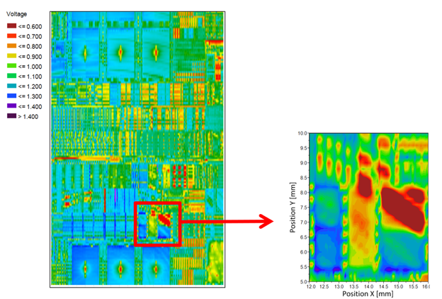
In addition, the FAaST platform provides flexible measurement capabilities that align with customer requirements. Manufacturers can perform rapid full-wafer characterization to monitor overall process health or use higher-resolution measurements to investigate localized regions of interest, such as active areas and capacitors (Figure 3). This combination of throughput and resolution allows engineers to balance efficiency with detailed analysis across development and production use cases.

Figure 3: Intra-die surface voltage measurement with µm-resolution. Die size is ~16x30mm, while the zoom area is 4x5mm size
As advanced packaging continues to enable next-generation electronics, manufacturers will require process control solutions beyond traditional inspection and dimensional metrology. They will need actionable insights into the electrical conditions that influence yield, reliability, and manufacturability.
With the FAaST platform, manufacturers can monitor and control residual surface charge, helping accelerate process development, improve consistency, and enable a faster path to high-volume manufacturing.
After all, the next frontier in process control isn’t just visual—it’s electrical.
Roberto Fumagalli is a Product Marketing Manager at Onto Innovation.

You Have a Challenge? Let’s talk.
We’d love to connect with you.
Looking to learn more about our innovative solutions and capabilities? Our team of experts is ready to assist you. Reach out today and let’s starts a conversation about how we can help you achieve your goals.
Let’s Talk
"*" indicates required fields